

Bachelor thesis
.pdfBachelor Thesis Presentation
Development of 3D Model of the Floating Diffusion Region of CCD Array Output Unit
Vadim Pogoretskiy
Microand Nanoelectronics Department
St-Petersburg Electrotechnical University “LETI” &
St-Petersburg Central Research Institute “Electron”
Supervisor: Mikhail Chetvergov PhD
St-Petersburg 2012
OUTLINE
1)Purpose of the work ………………………(3)
2)CCD-array applications …………………..(4)
3)real output unit ……………………………..(5)
4)3D modeling in SILVACO TCAD ……….(6)
5)Simulated results …………………………..(7)
6)Conclusion …………………………………….(11)

Purpose of the work:
Development of technological 3D model of the floating diffusion region (FDR) of output unit in SILVACO TCAD and analysis of characteristics.
Tasks:
1)Study of the operation of CCD-arrays.
2)Study of method of 3D modeling in SILVACO TCAD.
3)Design of technological 3D model of FDR.
4)Development of electrophysical 3D model of FDR.
5)Analysis of simulated results for different topology of FDR:
C-V characteristics.
Electrical field density and charge carriers distribution.
6)Development of recommendations to technologists for optimization of FDR topology.
3
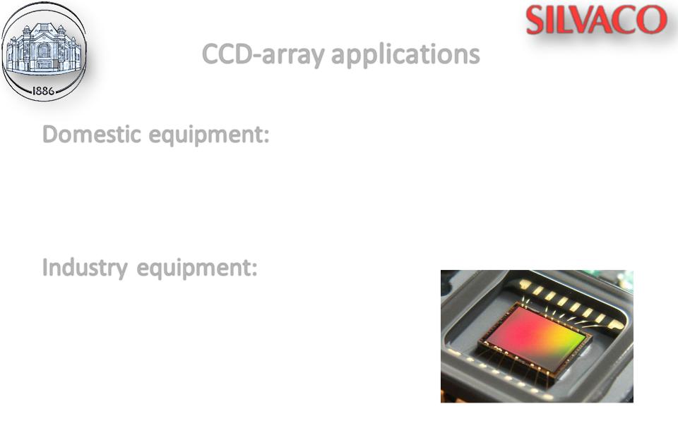
CCD-array applications
Domestic equipment:
Digital photo and video cameras
Telefaxes and scanners
Input optic devices
Industry equipment:
Movement sensors
Microscopy in medical and bio areas
Biometrical technologies
Spacecraft orientation
Earth remote sensing systems
Astronomical observes
Fig. 1. CCD - array
4
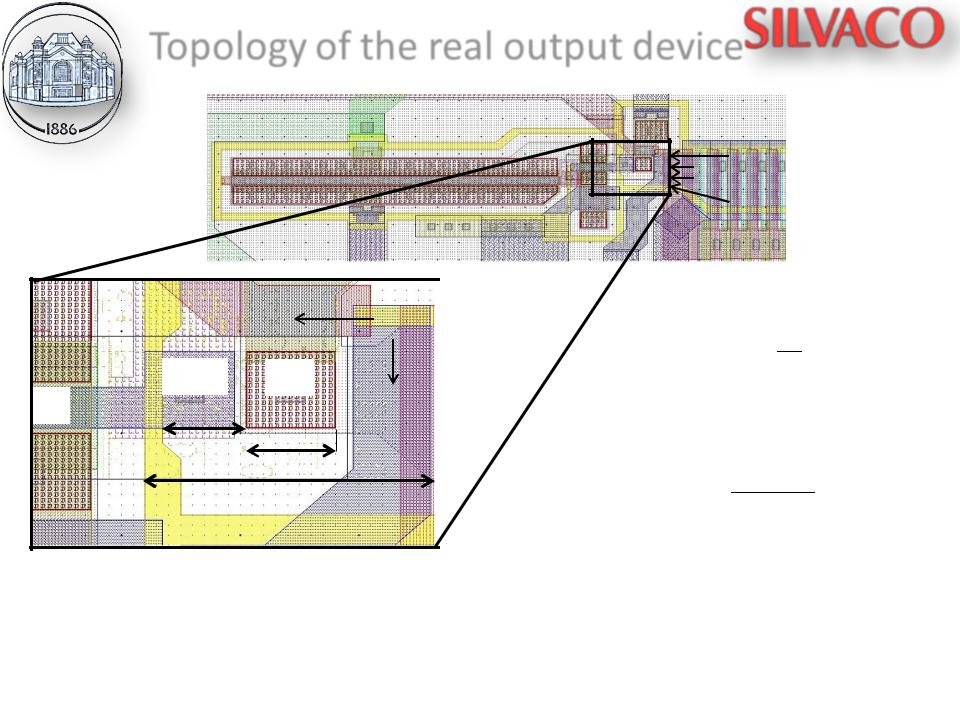
Topology of the real output device
|
|
|
|
|
|
4.5 µm |
|||
|
||||
|
|
|
6 µm |
|
|
|
|
18 µm |
|
|
|
|
|
|
|
|
|
stop-channel |
|
|
|
|
|
|
|
Fig. 2. |
|
Topology of 2- |
charge |
cascades |
packs |
output device |
|
|
|
|
|
|
|
|
|
|
|
|
|
|
|
|
|
|
|
|
|
|
|
|
|
|
|
|
|
|
|
|
|
|
|
|
|
|
|
|
|
|
|
|
|
= |
|
|
|
|||
|
|
|
|
|
|
|
|
|
||||
|
|
|
|
|
|
|
|
|
||||
|
|
|
|
|
|
|
|
|
|
Σ |
|
|
|
|
|
= |
+ |
|
|
|
+ |
+ |
|||
|
|
Σ |
|
|
|
|
|
|
|
|||
|
|
|
|
|
= |
ε |
ε |
|
|
|
|
|
|
|
|
|
0 |
|
Si |
|
|
||||
|
|
|
|
|
|
|
|
|||||
|
|
|
|
|
|
|
|
|||||
Table 1. solved values of capacitances and conversion slopes of FFD areas |
|
||||||
|
|
|
|
|
|
|
|
|
Area |
|
|
G+c |
Σ |
|
|
|
|
|
|
|
|
||
Capacitance of area , fF |
5-6 |
7−9 |
23−26 |
35−41 |
|
||
Conversion slope of area |
|
|
|
|
|
||
32-27 |
23-18 |
7-6 |
6-4 |
|
|||
k, |
µV |
5 |
|||||
|
|
|
|
||||
|
|
|
|
|
|
|
|
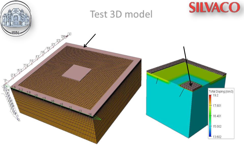
Test 3D model
Aluminum contact pad to the stop-channel:0 V
Aluminum contact pad to the n+ area: +15 V
p+
n+
p – substrate
Fig. 3. Dimension area |
Fig. 4. Doping distribution |
26 × 26 × 10 µm (grid) |
in the cut of structure |
6
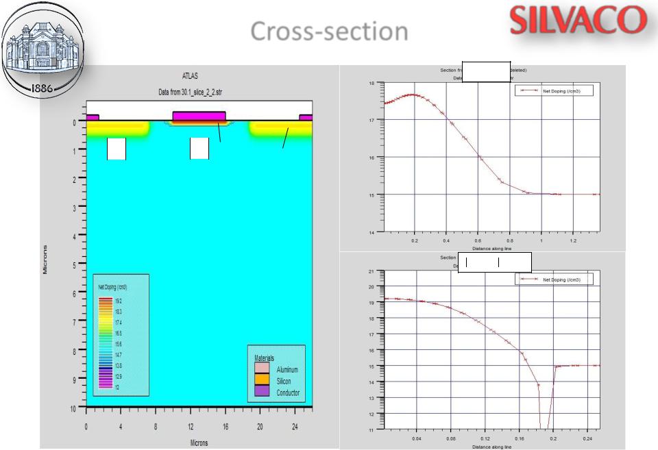
Cross-section
Na, sm-3
1 |
|
|
|
|
|
|
3 |
|
|||
|
|
|
|
|
|
|
|
|
|
|
|
2 |
|
4 n+ |
p+ |
|
|
|
|
|
|
(b)
p – substrate
Nd−Na , sm-3
(a)
(c)
Fig. 4. Doping distribution in the structure (a); cut 1-2 (b); cut 3-4 (c)
7

|
|
|
|
|
|
|
Simulated results |
|
|
|
|
|
|
|
|||||||
|
5 |
|
|
|
|
(a) |
|
|
|
|
|
|
|
|
|
|
(b) |
|
|
|
|
|
|
|
|
|
|
|
|
|
|
|
|
|
|
|
|
|
|
|
|
|
|
|
|
|
|
|
|
|
|
|
|
|
|
150 |
|
|
|
|
|
|
|
|
|
|
4 |
|
|
|
|
|
|
|
|
|
|
130 |
|
|
|
|
|
|
|
|
|
|
|
|
|
|
|
|
|
|
|
|
|
|
|
|
|
|
|
|
|
|
|
Capacitance, fF |
3 |
|
|
|
|
|
|
|
|
|
conversion slope, µV/electron |
110 |
|
|
|
|
|
|
|
|
|
|
|
|
|
|
|
|
|
|
|
|
|
|
|
|
|
|
|
|
|||
|
|
|
|
|
|
|
|
|
|
90 |
|
|
|
|
|
|
|
|
|
||
2 |
|
|
|
|
|
|
|
|
|
|
|
|
|
|
|
|
|
|
|
||
|
|
|
|
|
|
|
|
|
|
70 |
|
|
|
|
|
|
|
|
|
||
|
|
|
|
|
|
|
|
|
|
|
|
|
|
|
|
|
|
|
|
||
|
1 |
|
|
|
|
|
|
|
|
|
|
|
|
|
|
|
|
|
|
|
|
|
|
|
|
|
|
|
|
|
|
|
|
50 |
|
|
|
|
|
|
|
|
|
|
0 |
|
|
|
|
|
|
|
|
|
|
30 |
|
|
|
|
|
|
|
|
|
|
0 |
1 |
2 |
3 |
4 |
5 |
6 |
7 |
8 |
9 |
|
0 |
1 |
2 |
3 |
4 |
5 |
6 |
7 |
8 |
9 |
|
|
|
|
Distance between stop-n+, µm |
|
|
|
|
|
|
Distance between stop-n+, µm |
|
|
||||||||
|
|
|
|
|
|
|
|
|
|
|
|
|
|
|
|
|
|
||||
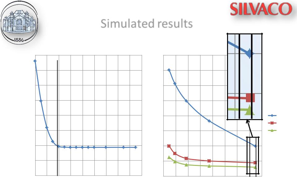
Fig. 5. Dependence of capacitance (а) and conversion slope (b) of FDR on distance between stop-channel and n+ area at 15 V
8
Emax, V/sm
Simulated results
8E+5 |
|
|
|
|
|
|
|
|
|
|
16 |
|
|
|
|
|
|
|
|
7E+5 |
|
|
|
|
|
|
|
|
|
|
14 |
|
|
|
|
|
|
|
|
6E+5 |
|
|
|
|
|
|
|
|
|
|
12 |
|
|
|
|
|
|
|
|
5E+5 |
|
|
|
|
|
|
|
|
|
fF |
10 |
|
|
|
|
|
|
|
|
|
|
|
|
|
|
|
|
|
|
|
|
|
|
|
|
|
|
|
|
4E+5 |
|
|
|
|
|
|
|
|
|
Capacitance, |
8 |
|
|
|
|
|
|
|
0 µм |
|
|
|
|
|
|
|
|
|
|
|
|
|
|
|
|
|
|||
|
|
|
|
|
|
|
|
|
|
|
|
|
|
|
|
|
|
|
3 µм |
3E+5 |
|
|
|
|
|
|
|
|
|
|
6 |
|
|
|
|
|
|
|
7.5 µм |
2E+5 |
|
|
|
|
|
|
|
|
|
|
4 |
|
|
|
|
|
|
|
|
1E+5 |
|
|
|
|
|
|
|
|
|
|
2 |
|
|
|
|
|
|
|
|
0E+0 |
|
|
|
|
|
|
|
|
|
|
0 |
|
|
|
|
|
|
|
|
0 |
1 |
2 |
3 |
4 |
5 |
6 |
7 |
8 |
9 |
|
0 |
2 |
4 |
6 |
8 |
10 |
12 |
14 |
16 |
Distance between stop-n+, µm |
Voltage, V |
|
Fig. 6. Dependence of maximum value of field density |
Fig. 7. C-V characteristics for different distances between |
in FDR on distance between stop-channel and n+ area |
stop-channel and n+ area |
at 15 V |
9 |

Visualization of modeling results
0 µ
0 µ
(а) |
(a) |
|
3 µ
3 µ
(b) |
(b) |
7.5 µ |
7.5 µ |
|
|
(c) |
(c) |
Fig. 8. Electrical field distribution in FDR |
Fig. 9. holes distribution in FDR |
distance between stop-channel and n+ area
(a) – 0 µ; (b) – 3 µ; (c) – 7.5 µ
10