


Chapter 4
Programmer’s Model for Test
This chapter describes the additional logic for functional verification and production testing. It contains the following sections:
•PrimeCell ACI test harness overview on page 4-2
•Scan testing on page 4-3
•Test registers on page 4-4.
ARM DDI 0146C |
© Copyright ARM Limited 1999. All rights reserved. |
4-1 |
Programmer’s Model for Test
4.1PrimeCell ACI test harness overview
The additional logic for functional verification and production testing allows:
•stimulation of input signals to the block
•capture of output signals
•generation of a special test clock enable signal to propagate test vectors.
These test features are controlled by test registers. This allows testing of the PrimeCell ACI in isolation from the rest of the system using only transfers from the APB.
Off-chip test vectors are supplied via a 32-bit parallel External Bus Interface (EBI) and converted to internal AMBA bus transfers. The application of test vectors is controlled via the Test Interface Controller (TIC) AMBA bus master module.
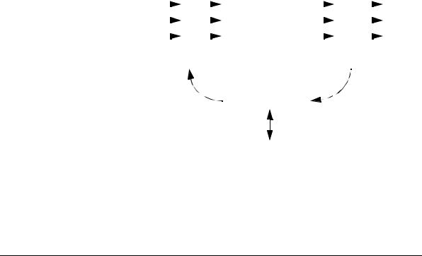
During test the ACICLK signal must be driven by the free-running PCLK clock signal so that the test vectors can be frequency independent. This clock multiplexing must be performed externally from the PrimeCell ACI. Figure 4-1 shows a block diagram of the PrimeCell ACI test harness.
Non- |
|
|
|
|
|
|
|
|
|
|
Non- |
|
|
|
|
|
|
|
|
|
|||
AMBA |
|
|
|
|
|
PrimeCell |
|
|
|
|
AMBA |
APB |
|
|
|
ACI |
|
|
|
|
APB |
||
Inputs |
|
|
|
|
|
|
|
|
|
|
Outputs |
|
|
|
|
|
|
|
|
|
|||
|
|
|
|
|
|
|
|
|
|
|
|
Test stimulus |
AMBA APB interface |
Test results |
|
|
capture |
|
|
Figure 4-1 PrimeCell ACI test harness
4-2 |
© Copyright ARM Limited 1999. All rights reserved. |
ARM DDI 0146C |

Programmer’s Model for Test
4.2Scan testing
The PrimeCell ACI has been designed to simplify the insertion of scan test cells and the use of Automatic Test Pattern Generation (ATPG) for an alternative method of manufacturing test.
During scan testing, the SCANMODE input must be driven HIGH to ensure that all internal data storage elements can be asynchronously reset. For normal use and application of manufacturing test vectors via the TIC, SCANMODE must be negated LOW.
ARM DDI 0146C |
© Copyright ARM Limited 1999. All rights reserved. |
4-3 |