


Functional Overview
2.3PrimeCell ACI operation
The operation of the PrimeCell Audio CODEC Interface is described in the following sections:
•Interface reset
•Clock signals
•PrimeCell ACI operation on page 2-8
•System loopback testing on page 2-10.
2.3.1Interface reset
The PrimeCell ACI is reset from the global reset signal BnRES and a block-specific reset signal nACIRST. An external reset controller must use BnRES to assert nACIRST asynchronously and negate it synchronously to ACICLK. BnRES should be asserted LOW, for a period long enough to reset the slowest block in the on-chip system, and then taken HIGH again. The ACI requires BnRES to be asserted LOW for at least one period of PCLK and nACIRST to be asserted LOW for at least one cycle of ACICLK.
The values of the registers after reset are detailed in Table 3-1 on page 3-3.
2.3.2Clock signals
The frequency of the input clock signal ACICLK, should be selected to generate the required output bit clock frequency for the ACIBITCLK signal to the off-chip CODEC device. An appropriate 10-bit divisor value CDLDVAL, must be programmed in the clock divider registers ACICDR_H and ACICDR_L. Program ACICDR_L with the least significant eight bits, and the ACICDR_H with the most significant two bits of the 10-bit divisor value.
The bit clock frequency is derived as follows:
F |
FAC ICLK |
|
ACIBITCLK = |
||
--------N---------- |
||
|
||
where: |
|
FACIBITCLK is the frequency of ACIBITCLK
FACICLK is the frequency of ACICLK
N is the divisor.
CDLDVAL = N - 1
Programming a zero value for CDLDVAL is not allowed.
ARM DDI 0146C |
© Copyright ARM Limited 1999. All rights reserved. |
2-7 |

Functional Overview
Programming CDLDVAL with a range of values from 1 to 1023 results in division of ACICLK by 2 to 1024.
For example, assuming an input clock ACICLK with frequency 18.432MHz, then:
CDLDVAL = 1 produces divide-by-2, FACIBITCLK = 8.216MHz (maximum)
CDLDVAL = 287 produces divide-by-288, FACIBITCLK = 64kHz
CDLDVAL = 1023 produces divide-by-1024, FACIBITCLK = 18kHz (minimum).
There is also a constraint on the ratio of clock frequencies for PCLK to ACICLK. The frequency of ACICLK must be less than, or equal to, two times the frequency of
PCLK:
FACICLK <= 2 x FPCLK
This is in order to guarantee that the received data byte is written to the FIFO before reception of the next data byte value.
The frequency of ACICLK may be less than PCLK and there are no constraints on the clock frequency ratio.
ACICLK may be driven with the PCLK signal if the frequency value is suitable for the output bit clock frequency. However, separate clock signals are often required due to other system constraints.
2.3.3PrimeCell ACI operation
Transmit and receive modes are enabled by programming either the TXEN and/or the RXEN bits to HIGH respectively in the control register (ACICR).
Note
Both receive and transmit modes are inhibited until a non-zero frequency clock divisor value has been written to the clock divider register (ACICDR_L and ACICDR_H).
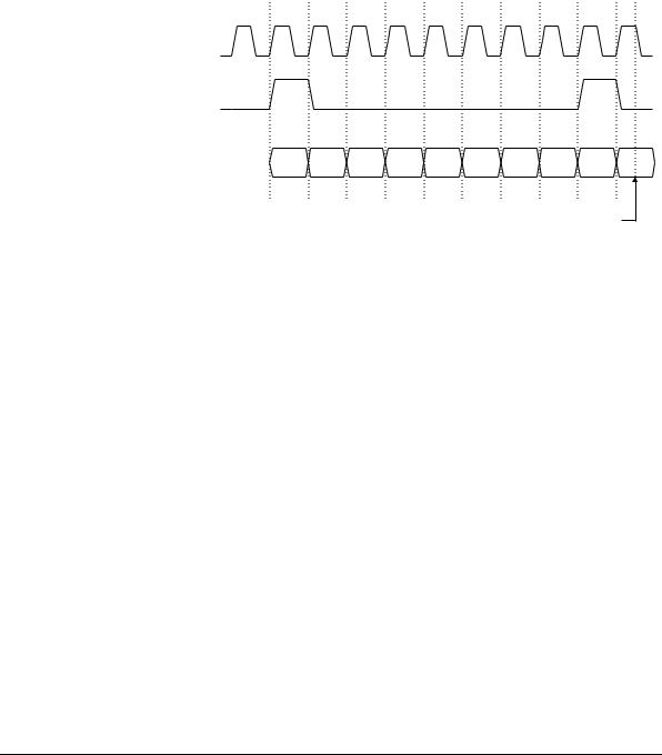
Data values are loaded into the transmit FIFO by writing to the data register (ACIDR). At the beginning of a transmit cycle, these data values are loaded into the transmit shift register, where they are shifted out serially on ACIDATAOUT, MSB first, with ACIFSYNC asserted during the first bit to indicate the start of the data frame. Data values are synchronous to the rising edge of ACIBITCLK. Figure 2-2 on page 2-9 shows this operation graphically.
2-8 |
© Copyright ARM Limited 1999. All rights reserved. |
ARM DDI 0146C |
Functional Overview
ACIBITCLK
ACIFSYNC
ACIDATAOUT /
ACIDATAIN
bit |
7 |
6 |
5 |
4 |
3 |
2 |
1 |
0 |
|
MSB |
|
|
|
|
|
|
LSB |
Receive data sampled on falling ACIBITCLK
Figure 2-2 PrimeCell ACI data input/output waveforms
Data values on ACIDATAIN are sampled on the falling edge of ACIBITCLK. The data bits are serially loaded into the receive shift register. When the complete byte has been received the data values are written into the receive FIFO. The status flags RXFE/ RXFF (receive FIFO empty/full), and TXFE/TXFF (transmit FIFO empty/full) indicate the FIFO level status. These flags can be monitored by reading the ACI Status Register (ACISR).
There are two internal interrupt signals that assert an active HIGH interrupt on ACITXINTR (when the transmit FIFO is less than half full), and on ACIRXINTR (when the receive FIFO is greater than or equal to half full). These interrupts are used to indicate that there is room for at least eight bytes in the transmit FIFO, and that eight bytes have been received, and can be read from the receive FIFO. The interrupts are cleared by filling or emptying the FIFOs as necessary. A combined interrupt output is also available that is generated as an OR function of the above two individual interrupts.
The microcontroller should use the transmit interrupt request to write transmit data at a sufficient rate to prevent an underflow error condition where the transmit FIFO becomes empty. If an underflow occurs invalid data (0x00) will be transmitted until the FIFO becomes non-empty or until transmit is disabled.
The microcontroller should use the receive interrupt request to read receive data at a sufficient rate to prevent an overflow error condition where the receive FIFO becomes full. If an overflow occurs then subsequent data will be lost until the FIFO is no longer full or until receive overflow has occurred.
ARM DDI 0146C |
© Copyright ARM Limited 1999. All rights reserved. |
2-9 |

Functional Overview
When all the transmit data values have been written to the ACI then TXEN can be negated LOW in ACICR. However, transmission will continue until the transmit FIFO and shift register are both empty. TXBUSY in ACISR will return a HIGH to indicate that the ACI transmit logic is busy. When a read of TXBUSY returns a LOW, then all the transmit data values have been sent and the transmit logic is no longer busy.
To end data reception, RXEN is negated LOW in ACICR. Reception will continue until the end of the current serial data frame and the data byte has been written to the receive FIFO. A read of RXBUSY in ACISR will return a HIGH while the receive logic is busy. Once the final data byte has been written to the receive FIFO then RXBUSY is negated LOW to indicate that the receive logic is no longer busy. The receive FIFO should now be read until empty.
2.3.4System loopback testing
A loopback test mode is available for system testing so that data transmitted on ACIDATAOUT can also be received on ACIDATAIN. Loopback mode is entered when a 1 is written to the LOOP bit in ACICR. For normal operation the LOOP bit must always be 0, which is also the default state at reset.
2-10 |
© Copyright ARM Limited 1999. All rights reserved. |
ARM DDI 0146C |