

- •Features
- •1. Pin Configurations
- •1.1 Pin Descriptions
- •1.1.3 Port A (PA2..PA0)
- •1.1.4 Port B (PB7..PB0)
- •1.1.5 Port D (PD6..PD0)
- •1.1.6 RESET
- •1.1.7 XTAL1
- •1.1.8 XTAL2
- •2. Overview
- •2.1 Block Diagram
- •2.2 Comparison Between ATtiny2313A and ATtiny4313
- •3. About
- •3.1 Resources
- •3.2 Code Examples
- •3.3 Data Retention
- •4. CPU Core
- •4.1 Architectural Overview
- •4.2 ALU – Arithmetic Logic Unit
- •4.3 Status Register
- •4.4 General Purpose Register File
- •4.5 Stack Pointer
- •4.6 Instruction Execution Timing
- •4.7 Reset and Interrupt Handling
- •4.7.1 Interrupt Response Time
- •5. Memories
- •5.1 Program Memory (Flash)
- •5.2 Data Memory (SRAM) and Register Files
- •5.2.1 General Purpose Register File
- •5.2.2 I/O Register File
- •5.2.3 Data Memory (SRAM)
- •5.3 Data Memory (EEPROM)
- •5.3.1 Programming Methods
- •5.3.2 Read
- •5.3.3 Erase
- •5.3.4 Write
- •5.3.5 Preventing EEPROM Corruption
- •5.3.6 Program Examples
- •5.4 Register Description
- •5.4.1 EEAR – EEPROM Address Register
- •5.4.2 EEDR – EEPROM Data Register
- •5.4.3 EECR – EEPROM Control Register
- •5.4.4 GPIOR2 – General Purpose I/O Register 2
- •5.4.5 GPIOR1 – General Purpose I/O Register 1
- •5.4.6 GPIOR0 – General Purpose I/O Register 0
- •6. Clock System
- •6.1 Clock Subsystems
- •6.2 Clock Sources
- •6.2.1 Default Clock Source
- •6.2.2 External Clock
- •6.2.3 Calibrated Internal RC Oscillator
- •6.2.4 128 kHz Internal Oscillator
- •6.2.5 Crystal Oscillator
- •6.3 System Clock Prescaler
- •6.3.1 Switching Time
- •6.4 Clock Output Buffer
- •6.5 Register Description
- •6.5.1 OSCCAL – Oscillator Calibration Register
- •6.5.2 CLKPR – Clock Prescale Register
- •7. Power Management and Sleep Modes
- •7.1 Sleep Modes
- •7.1.1 Idle Mode
- •7.1.3 Standby Mode
- •7.2 Software BOD Disable
- •7.3 Power Reduction Register
- •7.4 Minimizing Power Consumption
- •7.4.1 Analog Comparator
- •7.4.2 Internal Voltage Reference
- •7.4.4 Watchdog Timer
- •7.4.5 Port Pins
- •7.5 Register Description
- •7.5.1 MCUCR – MCU Control Register
- •7.5.2 PRR – Power Reduction Register
- •8. System Control and Reset
- •8.1 Resetting the AVR
- •8.2 Reset Sources
- •8.2.2 External Reset
- •8.2.4 Watchdog Reset
- •8.3 Internal Voltage Reference
- •8.4 Watchdog Timer
- •8.4.1 Timed Sequences for Changing the Configuration of the Watchdog Timer
- •8.4.2 Code Example
- •8.5 Register Description
- •8.5.1 MCUSR – MCU Status Register
- •8.5.2 WDTCSR – Watchdog Timer Control and Status Register
- •9. Interrupts
- •9.1 Interrupt Vectors
- •9.2 External Interrupts
- •9.2.1 Low Level Interrupt
- •9.2.2 Pin Change Interrupt Timing
- •9.3 Register Description
- •9.3.1 MCUCR – MCU Control Register
- •9.3.2 GIMSK – General Interrupt Mask Register
- •9.3.3 GIFR – General Interrupt Flag Register
- •9.3.4 PCMSK2 – Pin Change Mask Register 2
- •9.3.5 PCMSK1 – Pin Change Mask Register 1
- •9.3.6 PCMSK0 – Pin Change Mask Register 0
- •10. I/O-Ports
- •10.1 Ports as General Digital I/O
- •10.1.1 Configuring the Pin
- •10.1.2 Toggling the Pin
- •10.1.3 Switching Between Input and Output
- •10.1.4 Reading the Pin Value
- •10.1.5 Digital Input Enable and Sleep Modes
- •10.1.6 Unconnected Pins
- •10.1.7 Program Examples
- •10.2 Alternate Port Functions
- •10.2.1 Alternate Functions of Port A
- •10.2.2 Alternate Functions of Port B
- •10.2.3 Alternate Functions of Port D
- •10.3 Register Description
- •10.3.1 MCUCR – MCU Control Register
- •10.3.2 PORTA – Port A Data Register
- •10.3.3 DDRA – Port A Data Direction Register
- •10.3.4 PINA – Port A Input Pins Address
- •10.3.5 PORTB – Port B Data Register
- •10.3.6 DDRB – Port B Data Direction Register
- •10.3.7 PINB – Port B Input Pins Address
- •10.3.8 PORTD – Port D Data Register
- •10.3.9 DDRD – Port D Data Direction Register
- •10.3.10 PIND – Port D Input Pins Address
- •11. 8-bit Timer/Counter0 with PWM
- •11.1 Features
- •11.2 Overview
- •11.2.1 Registers
- •11.2.2 Definitions
- •11.3 Clock Sources
- •11.4 Counter Unit
- •11.5 Output Compare Unit
- •11.5.1 Force Output Compare
- •11.5.2 Compare Match Blocking by TCNT0 Write
- •11.5.3 Using the Output Compare Unit
- •11.6 Compare Match Output Unit
- •11.6.1 Compare Output Mode and Waveform Generation
- •11.7 Modes of Operation
- •11.7.1 Normal Mode
- •11.7.2 Clear Timer on Compare Match (CTC) Mode
- •11.7.3 Fast PWM Mode
- •11.7.4 Phase Correct PWM Mode
- •11.8 Timer/Counter Timing Diagrams
- •11.9 Register Description
- •11.9.1 TCCR0A – Timer/Counter Control Register A
- •11.9.2 TCCR0B – Timer/Counter Control Register B
- •11.9.3 TCNT0 – Timer/Counter Register
- •11.9.4 OCR0A – Output Compare Register A
- •11.9.5 OCR0B – Output Compare Register B
- •11.9.6 TIMSK – Timer/Counter Interrupt Mask Register
- •11.9.7 TIFR – Timer/Counter Interrupt Flag Register
- •12. 16-bit Timer/Counter1
- •12.1 Features
- •12.2 Overview
- •12.2.1 Registers
- •12.2.2 Definitions
- •12.2.3 Compatibility
- •12.3 Timer/Counter Clock Sources
- •12.4 Counter Unit
- •12.5 Input Capture Unit
- •12.5.1 Input Capture Trigger Source
- •12.5.2 Noise Canceler
- •12.5.3 Using the Input Capture Unit
- •12.6 Output Compare Units
- •12.6.1 Force Output Compare
- •12.6.2 Compare Match Blocking by TCNT1 Write
- •12.6.3 Using the Output Compare Unit
- •12.7 Compare Match Output Unit
- •12.7.1 Compare Output Mode and Waveform Generation
- •12.8 Modes of Operation
- •12.8.1 Normal Mode
- •12.8.2 Clear Timer on Compare Match (CTC) Mode
- •12.8.3 Fast PWM Mode
- •12.8.4 Phase Correct PWM Mode
- •12.8.5 Phase and Frequency Correct PWM Mode
- •12.9 Timer/Counter Timing Diagrams
- •12.10 Accessing 16-bit Registers
- •12.10.1 Reusing the Temporary High Byte Register
- •12.11 Register Description
- •12.11.1 TCCR1A – Timer/Counter1 Control Register A
- •12.11.2 TCCR1B – Timer/Counter1 Control Register B
- •12.11.3 TCCR1C – Timer/Counter1 Control Register C
- •12.11.4 TCNT1H and TCNT1L – Timer/Counter1
- •12.11.5 OCR1AH and OCR1AL – Output Compare Register 1 A
- •12.11.6 OCR1BH and OCR1BL – Output Compare Register 1 B
- •12.11.7 ICR1H and ICR1L – Input Capture Register 1
- •12.11.8 TIMSK – Timer/Counter Interrupt Mask Register
- •12.11.9 TIFR – Timer/Counter Interrupt Flag Register
- •13. Timer/Counter0 and Timer/Counter1 Prescalers
- •13.1 Internal Clock Source
- •13.2 Prescaler Reset
- •13.3 External Clock Source
- •13.4 Register Description
- •13.4.1 GTCCR – General Timer/Counter Control Register
- •14. USART
- •14.1 Features
- •14.2 Overview
- •14.2.1 AVR USART vs. AVR UART – Compatibility
- •14.3 Clock Generation
- •14.3.1 Internal Clock Generation – The Baud Rate Generator
- •14.3.2 Double Speed Operation (U2X)
- •14.3.3 External Clock
- •14.3.4 Synchronous Clock Operation
- •14.4 Frame Formats
- •14.4.1 Parity Bit Calculation
- •14.5 USART Initialization
- •14.6 Data Transmission – The USART Transmitter
- •14.6.1 Sending Frames with 5 to 8 Data Bit
- •14.6.2 Sending Frames with 9 Data Bit
- •14.6.3 Transmitter Flags and Interrupts
- •14.6.4 Parity Generator
- •14.6.5 Disabling the Transmitter
- •14.7 Data Reception – The USART Receiver
- •14.7.1 Receiving Frames with 5 to 8 Data Bits
- •14.7.2 Receiving Frames with 9 Data Bits
- •14.7.3 Receive Compete Flag and Interrupt
- •14.7.4 Receiver Error Flags
- •14.7.5 Parity Checker
- •14.7.6 Disabling the Receiver
- •14.7.7 Flushing the Receive Buffer
- •14.8 Asynchronous Data Reception
- •14.8.1 Asynchronous Clock Recovery
- •14.8.2 Asynchronous Data Recovery
- •14.8.3 Asynchronous Operational Range
- •14.9.1 Using MPCM
- •14.10 Register Description
- •14.10.1 UDR – USART I/O Data Register
- •14.10.2 UCSRA – USART Control and Status Register A
- •14.10.3 UCSRB – USART Control and Status Register B
- •14.10.4 UCSRC – USART Control and Status Register C
- •14.10.5 UBRRL and UBRRH – USART Baud Rate Registers
- •14.11 Examples of Baud Rate Setting
- •15. USART in SPI Mode
- •15.1 Features
- •15.2 Overview
- •15.3 Clock Generation
- •15.4 SPI Data Modes and Timing
- •15.5 Frame Formats
- •15.5.1 USART MSPIM Initialization
- •15.6 Data Transfer
- •15.6.1 Transmitter and Receiver Flags and Interrupts
- •15.6.2 Disabling the Transmitter or Receiver
- •15.7 AVR USART MSPIM vs. AVR SPI
- •15.8 Register Description
- •15.8.1 UDR – USART MSPIM I/O Data Register
- •15.8.2 UCSRA – USART MSPIM Control and Status Register A
- •15.8.3 UCSRB – USART MSPIM Control and Status Register B
- •15.8.4 UCSRC – USART MSPIM Control and Status Register C
- •15.8.5 UBRRL and UBRRH – USART MSPIM Baud Rate Registers
- •16. USI – Universal Serial Interface
- •16.1 Features
- •16.2 Overview
- •16.3 Functional Descriptions
- •16.3.2 SPI Master Operation Example
- •16.3.3 SPI Slave Operation Example
- •16.3.5 Start Condition Detector
- •16.3.6 Clock speed considerations
- •16.4 Alternative USI Usage
- •16.4.4 Edge Triggered External Interrupt
- •16.4.5 Software Interrupt
- •16.5 Register Description
- •16.5.1 USICR – USI Control Register
- •16.5.2 USISR – USI Status Register
- •16.5.3 USIDR – USI Data Register
- •16.5.4 USIBR – USI Buffer Register
- •17. Analog Comparator
- •17.1 Register Description
- •17.1.1 ACSR – Analog Comparator Control and Status Register
- •17.1.2 DIDR – Digital Input Disable Register
- •18. debugWIRE On-chip Debug System
- •18.1 Features
- •18.2 Overview
- •18.3 Physical Interface
- •18.4 Software Break Points
- •18.5 Limitations of debugWIRE
- •18.6 Register Description
- •18.6.1 DWDR – debugWire Data Register
- •19. Self-Programming
- •19.1 Features
- •19.2 Overview
- •19.3 Lock Bits
- •19.4.2 Page Erase
- •19.4.3 Page Load
- •19.4.4 Page Write
- •19.4.5 SPMCSR Can Not Be Written When EEPROM is Programmed
- •19.5 Preventing Flash Corruption
- •19.6 Programming Time for Flash when Using SPM
- •19.7 Register Description
- •19.7.1 SPMCSR – Store Program Memory Control and Status Register
- •20. Lock Bits, Fuse Bits and Device Signature
- •20.1 Lock Bits
- •20.2 Fuse Bits
- •20.2.1 Latching of Fuses
- •20.3 Device Signature Imprint Table
- •20.3.1 Calibration Byte
- •20.3.2 Signature Bytes
- •20.4 Reading Lock Bits, Fuse Bits and Signature Data from Software
- •20.4.1 Lock Bit Read
- •20.4.2 Fuse Bit Read
- •20.4.3 Device Signature Imprint Table Read
- •21. External Programming
- •21.1 Memory Parametrics
- •21.2 Parallel Programming
- •21.2.1 Enter Programming Mode
- •21.2.2 Considerations for Efficient Programming
- •21.2.3 Chip Erase
- •21.2.4 Programming the Flash
- •21.2.5 Programming the EEPROM
- •21.2.6 Reading the Flash
- •21.2.7 Reading the EEPROM
- •21.2.8 Programming Low Fuse Bits
- •21.2.9 Programming High Fuse Bits
- •21.2.10 Programming Extended Fuse Bits
- •21.2.11 Programming the Lock Bits
- •21.2.12 Reading Fuse and Lock Bits
- •21.2.13 Reading Signature Bytes
- •21.2.14 Reading the Calibration Byte
- •21.3 Serial Programming
- •21.3.1 Pin Mapping
- •21.3.2 Programming Algorithm
- •21.3.3 Programming Instruction Set
- •21.4 Programming Time for Flash and EEPROM
- •22. Electrical Characteristics
- •22.1 Absolute Maximum Ratings*
- •22.2 DC Characteristics
- •22.3 Speed
- •22.4 Clock Characteristics
- •22.4.1 Calibrated Internal RC Oscillator Accuracy
- •22.4.2 External Clock Drive
- •22.5 System and Reset Characteristics
- •22.6 Analog Comparator Characteristics
- •22.7 Parallel Programming Characteristics
- •22.8 Serial Programming Characteristics
- •23. Typical Characteristics
- •23.1 Effect of Power Reduction
- •23.2 ATtiny2313A
- •23.2.1 Current Consumption in Active Mode
- •23.2.2 Current Consumption in Idle Mode
- •23.2.4 Current Consumption in Reset
- •23.2.5 Current Consumption of Peripheral Units
- •23.2.7 Output Driver Strength
- •23.2.8 Input Thresholds and Hysteresis (for I/O Ports)
- •23.2.9 BOD, Bandgap and Reset
- •23.2.10 Internal Oscillator Speed
- •23.3 ATtiny4313
- •23.3.1 Current Consumption in Active Mode
- •23.3.2 Current Consumption in Idle Mode
- •23.3.4 Current Consumption in Reset
- •23.3.5 Current Consumption of Peripheral Units
- •23.3.7 Output Driver Strength
- •23.3.8 Input Thresholds and Hysteresis (for I/O Ports)
- •23.3.9 BOD, Bandgap and Reset
- •23.3.10 Internal Oscillator Speed
- •24. Register Summary
- •25. Instruction Set Summary
- •26. Ordering Information
- •26.1 ATtiny2313A
- •26.2 ATtiny4313
- •27. Packaging Information
- •28. Errata
- •28.1 ATtiny2313A
- •28.2 ATtiny4313
- •29. Datasheet Revision History
- •Table of Contents
8.2Reset Sources
The ATtiny2313A/4313 has four sources of reset:
•Power-on Reset. The MCU is reset when the supply voltage is below the Power-on Reset threshold (VPOT)
•External Reset. The MCU is reset when a low level is present on the RESET pin for longer than the minimum pulse length when RESET function is enabled
•Watchdog Reset. The MCU is reset when the Watchdog Timer period expires and the Watchdog is enabled
•Brown-out Reset. The MCU is reset when the supply voltage VCC is below the Brown-out Reset threshold (VBOT) and the Brown-out Detector is enabled
8.2.1Power-on Reset
A Power-on Reset (POR) pulse is generated by an on-chip detection circuit. The detection level is defined in “System and Reset Characteristics” on page 201. The POR is activated whenever VCC is below the detection level. The POR circuit can be used to trigger the Start-up Reset, as well as to detect a failure in supply voltage.
A Power-on Reset (POR) circuit ensures that the device is reset from Power-on. Reaching the Power-on Reset threshold voltage invokes the delay counter, which determines how long the device is kept in reset after VCC rise. The reset signal is activated again, without any delay, when VCC decreases below the detection level.
Figure 8-2. MCU Start-up, RESET Tied to VCC
|
VCC |
|
VPOT |
|
||||
|
|
|
|
|
|
|
||
|
|
|
|
VRST |
|
|||
|
RESET |
|
||||||
|
|
|
|
|
|
|
||
TIME-OUT |
|
|
tTOUT |
|
|
|
||
|
|
|
|
|
||||
|
|
|
|
|
||||
INTERNAL
RESET
Figure 8-3. MCU Start-up, RESET Extended Externally
VPOT
VCC
VRST
RESET
tTOUT
TIME-OUT
INTERNAL
RESET
40 ATtiny2313A/4313
8246B–AVR–09/11
 ATtiny2313A/4313
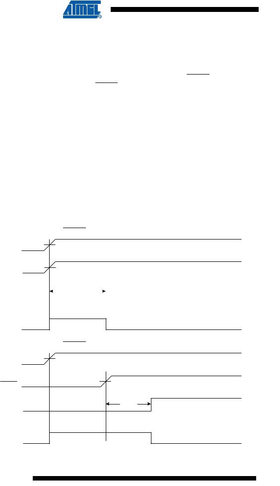
8.2.2External Reset
An External Reset is generated by a low level on the RESET pin if enabled. Reset pulses longer than the minimum pulse width (see “System and Reset Characteristics” on page 201) will generate a reset, even if the clock is not running. Shorter pulses are not guaranteed to generate a reset. When the applied signal reaches the Reset Threshold Voltage – VRST – on its positive edge, the delay counter starts the MCU after the Time-out period – tTOUT – has expired.
Figure 8-4. External Reset During Operation
 CC
CC
8.2.3Brown-out Detection
ATtiny2313A/4313 has an On-chip Brown-out Detection (BOD) circuit for monitoring the VCC level during operation by comparing it to a fixed trigger level. The trigger level for the BOD can be selected by the BODLEVEL Fuses. The trigger level has a hysteresis to ensure spike free Brown-out Detection. The hysteresis on the detection level should be interpreted as VBOT+ =
VBOT + VHYST/2 and VBOT- = VBOT - VHYST/2.
When the BOD is enabled, and VCC decreases to a value below the trigger level (VBOT- in Figure 8-5 on page 41), the Brown-out Reset is immediately activated. When VCC increases above the
trigger level (VBOT+ in Figure 8-5 on page 41), the delay counter starts the MCU after the Timeout period tTOUT has expired.
The BOD circuit will only detect a drop in VCC if the voltage stays below the trigger level for longer than tBOD given in “System and Reset Characteristics” on page 201.
Figure 8-5. Brown-out Reset During Operation
VCC |
VBOT+ |
|
VBOT- |
RESET
TIME-OUT |
tTOUT |
INTERNAL
RESET
41
8246B–AVR–09/11