

 ATmega128
Pin
Configurations
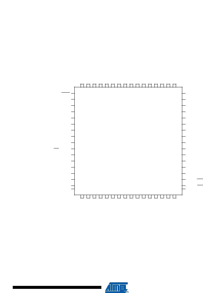
Figure 1. Pinout ATmega128
AVCC |
GND |
AREF |
PF0 (ADC0) |
PF1 (ADC1) |
PF2 (ADC2) |
PF3 (ADC3) |
PF4 (ADC4/TCK) |
PF5 (ADC5/TMS) |
PF6 (ADC6/TDO) |
PF7 (ADC7/TDI) |
GND |
VCC |
PA0 (AD0) |
PA1 (AD1) |
PA2 (AD2) |
PEN RXD0/(PDI) PE0 (TXD0/PDO) PE1 (XCK0/AIN0) PE2 (OC3A/AIN1) PE3 (OC3B/INT4) PE4 (OC3C/INT5) PE5
(T3/INT6) PE6 (ICP3/INT7) PE7 (SS) PB0 (SCK) PB1 (MOSI) PB2 (MISO) PB3 (OC0) PB4 (OC1A) PB5 (OC1B) PB6
64 
 1
1 

 2
2

 3
3

 4
4

 5
5

 6
6

 7
7

 8
8

 9
9

 10
10

 11
11

 12
12

 13
13

 14
14

 15
15

 16 17
16 17
PB7(OC2/OC1C)
63
TOSC2/PG3 18
62 |
61 |
60 |
59 |
58 |
57 |
56 |
55 |
54 |
53 |
52 |
51 |
50 |
19 |
20 |
21 |
22 |
23 |
24 |
25 |
26 |
27 |
28 |
29 |
30 |
31 |
|
TOSC1/PG4 |
|
RESET |
VCC |
GND |
XTAL2 |
XTAL1 |
(SCL/INT0) PD0 |
(SDA/INT1) PD1 |
(RXD1/INT2) PD2 |
(TXD1/INT3) PD3 |
(ICP1) PD4 |
(XCK1) PD5 |
(T1) PD6 |
|
|||||||||||||
|
|
|
|
|
|||||||||
49 48  PA3 (AD3)
47  PA4 (AD4)
46  PA5 (AD5)
45  PA6 (AD6)
44  PA7 (AD7)
43  PG2(ALE)
42  PC7 (A15)
41  PC6 (A14)
40  PC5 (A13)
39  PC4 (A12)
38  PC3 (A11)
37  PC2 (A10)
36  PC1 (A9)
35  PC0 (A8)
34  PG1(RD)
33 
 PG0(WR) 32
PD7(T2)
Note: The Pinout figure applies to both TQFP and MLF packages. The bottom pad under the QFN/MLF package should be soldered to ground.
Overview
The ATmega128 is a low-power CMOS 8-bit microcontroller based on the AVR enhanced RISC architecture. By executing powerful instructions in a single clock cycle, the ATmega128 achieves throughputs approaching 1 MIPS per MHz allowing the system designer to optimize power consumption versus processing speed.
2
2464US–AVR–08/10

ATmega128
Block Diagram
Figure 2. Block Diagram
PF0 - PF7 |
PA0 - PA7 |
PC0 - PC7 |
VCC
GND
|
|
|
|
|
PORTF DRIVERS |
|
|
|
|
|
|
PORTA DRIVERS |
|
|
|
|
|
|
PORTC DRIVERS |
||||||||||||||||||||||||||||||||||||||||
|
|
|
|
|
|
|
|
|
|
|
|
|
|
|
|
|
|
|
|
|
|
|
|
|
|
|
|
|
|
|
|
|
|
|
|
|
|
|
|
|
|
|
|
|
|
|
|
|
|
|
|
|
|
|
|
|
|
|
|
|
|
|
|
|
|
|
|
|
|
|
|
|
|
|
|
|
|
|
|
|
|
|
|
|
|
|
|
|
|
|
|
|
|
|
|
|
|
|
|
|
|
|
|
|
|
|
|
|
|
|
|
|
|
|
|
|
|
|
|
|
|
|
|
|
|
|
|
|
|
|
|
|
|
|
|
|
|
|
|
|
|
|
|
|
|
|
|
|
|
|
|
|
|
|
|
|
|
|
|
|
|
|
|
|
|
|
|
|
|
|
|
|
|
|
|
|
|
|
|
|
|
|
|
|
|
|
|
|
|
|
|
|
|
|
|
|
|
|
|
|
|
|
|
|
|
|
|
|
|
|
|
|
|
|
|
|
|
|
|
|
|
|
|
|
|
|
|
|
|
|
|
|
|
|
|
|
|
|
|
DATA REGISTER |
|
|
|
DATA DIR. |
|
DATA REGISTER |
|
|
|
DATA DIR. |
|
DATA REGISTER |
|
|
|
DATA DIR. |
|||||||||||||||||||||||||||||||||||||||||||
|
|
PORTF |
|
|
REG. PORTF |
|
|
|
PORTA |
|
|
REG. PORTA |
|
|
|
PORTC |
|
|
REG. PORTC |
||||||||||||||||||||||||||||||||||||||||
8-BIT DATA BUS
|
|
|
|
|
|
RESET |
|
|
|
|
|
|
|
XTAL1 |
|
XTAL2 |
|
|||
|
||||||
AVCC |
|
|
|
|
|
|
|
|
CALIB. OSC |
|
|
|
|
|
|
|
|
|
|
INTERNAL |
|
|
|
||
AGND |
|
|
|
ADC |
|
|
|
|
|
|
||
|
|
|
|
|
OSCILLATOR |
|
|
|
|
|||
|
|
|
|
|
|
|
|
|
|
|
||
AREF |
|
|
|
|
|
|
|
|
OSCILLATOR |
|
|
|
|
|
|
|
|
|
|
|
|
|
|
|
|
|
|
JTAG TAP |
|
PROGRAM |
STACK |
|
WATCHDOG |
|
|
|
|
|
|
|
|
COUNTER |
POINTER |
|
|
TIMER |
|
|
|
|
|
|
|
|
|
|
|
OSCILLATOR |
|
|
|
|||
|
|
|
|
|
|
|
|
|
|
|
|
|
|
ON-CHIP DEBUG |
PROGRAM |
SRAM |
|
MCU CONTROL |
TIMING AND |
|
|
|
|||
|
FLASH |
|
|
REGISTER |
CONTROL |
|
|
|
||||
|
|
BOUNDARY- |
|
INSTRUCTION |
GENERAL |
|
|
TIMER/ |
|
|
|
|
|
|
SCAN |
|
|
|
|
|
|
|
|||
|
|
|
REGISTER |
|
COUNTERS |
|
|
|
|
|||
|
|
|
|
PURPOSE |
|
|
|
|
|
|||
|
|
|
|
|
|
|
|
|
|
|
|
|
|
|
|
|
|
REGISTERS |
|
|
|
|
|
|
|
|
PROGRAMMING |
|
X |
|
|
|
|
|
|
|
||
PEN |
INSTRUCTION |
Y |
|
INTERRUPT |
|
|
|
|
||||
|
LOGIC |
|
|
|
|
|
|
|||||
|
|
|
DECODER |
Z |
|
|
UNIT |
|
|
|
|
|
|
|
|
|
|
|
|
|
|
|
|||
|
|
|
|
CONTROL |
ALU |
|
|
EEPROM |
|
|
|
|
|
|
|
|
LINES |
|
|
|
|
|
|
||
|
|
|
|
|
|
|
|
|
|
|
|
|
|
|
|
|
|
STATUS |
|
|
|
|
|
|
|
|
|
|
|
|
REGISTER |
|
|
|
|
|
|
|
|
|
|
USART0 |
|
|
|
|
SPI |
USART1 |
TWO-WIRE SERIAL |
|
|
|
|
|
|
|
|
|
|
INTERFACE |
|
|||
|
|
|
|
|
|
|
|
|
|
|
|
|
|
ANALOG COMPARATOR |
DATA REGISTER |
DATA DIR. |
DATA REGISTER |
DATA DIR. |
DATA REGISTER |
DATA DIR. |
DATA REG. |
DATA DIR. |
|||
|
+ - |
PORTE |
REG. PORTE |
PORTB |
REG. PORTB |
PORTD |
REG. PORTD |
PORTG |
REG. PORTG |
|||
|
|
|
|
|
|
|
|
|
|
|
||
|
|
|
PORTE DRIVERS |
PORTB DRIVERS |
|
PORTD DRIVERS |
|
PORTG DRIVERS |
||||
|
|
|
PE0 - PE7 |
PB0 - PB7 |
|
PD0 - PD7 |
|
PG0 - PG4 |
||||
|
|
|
|
|
|
|
|
|
|
|
|
3 |
2464US–AVR–08/10 |
|
|
|
|
|
|
|
|
|
|
||

 ATmega128
ATmega103 and
ATmega128
Compatibility
The AVR core combines a rich instruction set with 32 general purpose working registers. All the 32 registers are directly connected to the Arithmetic Logic Unit (ALU), allowing two independent registers to be accessed in one single instruction executed in one clock cycle. The resulting architecture is more code efficient while achieving throughputs up to ten times faster than conventional CISC microcontrollers.
The ATmega128 provides the following features: 128 Kbytes of In-System Programmable Flash with Read-While-Write capabilities, 4 Kbytes EEPROM, 4 Kbytes SRAM, 53 general purpose I/O lines, 32 general purpose working registers, Real Time Counter (RTC), four flexible Timer/Counters with compare modes and PWM, 2 USARTs, a byte oriented Two-wire Serial Interface, an 8- channel, 10-bit ADC with optional differential input stage with programmable gain, programmable Watchdog Timer with Internal Oscillator, an SPI serial port, IEEE std. 1149.1 compliant JTAG test interface, also used for accessing the On-chip Debug system and programming and six software selectable power saving modes. The Idle mode stops the CPU while allowing the SRAM, Timer/Counters, SPI port, and interrupt system to continue functioning. The Power-down mode saves the register contents but freezes the Oscillator, disabling all other chip functions until the next interrupt or Hardware Reset. In Power-save mode, the asynchronous timer continues to run, allowing the user to maintain a timer base while the rest of the device is sleeping. The ADC Noise Reduction mode stops the CPU and all I/O modules except Asynchronous Timer and ADC, to minimize switching noise during ADC conversions. In Standby mode, the Crystal/Resonator Oscillator is running while the rest of the device is sleeping. This allows very fast start-up combined with low power consumption. In Extended Standby mode, both the main Oscillator and the Asynchronous Timer continue to run.
The device is manufactured using Atmel’s high-density nonvolatile memory technology. The Onchip ISP Flash allows the program memory to be reprogrammed in-system through an SPI serial interface, by a conventional nonvolatile memory programmer, or by an On-chip Boot program running on the AVR core. The boot program can use any interface to download the application program in the application Flash memory. Software in the Boot Flash section will continue to run while the Application Flash section is updated, providing true Read-While-Write operation. By combining an 8-bit RISC CPU with In-System Self-Programmable Flash on a monolithic chip, the Atmel ATmega128 is a powerful microcontroller that provides a highly flexible and cost effective solution to many embedded control applications.
The ATmega128 AVR is supported with a full suite of program and system development tools including: C compilers, macro assemblers, program debugger/simulators, in-circuit emulators, and evaluation kits.
The ATmega128 is a highly complex microcontroller where the number of I/O locations supersedes the 64 I/O locations reserved in the AVR instruction set. To ensure backward compatibility with the ATmega103, all I/O locations present in ATmega103 have the same location in ATmega128. Most additional I/O locations are added in an Extended I/O space starting from $60 to $FF, (i.e., in the ATmega103 internal RAM space). These locations can be reached by using LD/LDS/LDD and ST/STS/STD instructions only, not by using IN and OUT instructions. The relocation of the internal RAM space may still be a problem for ATmega103 users. Also, the increased number of interrupt vectors might be a problem if the code uses absolute addresses. To solve these problems, an ATmega103 compatibility mode can be selected by programming the fuse M103C. In this mode, none of the functions in the Extended I/O space are in use, so the internal RAM is located as in ATmega103. Also, the Extended Interrupt vectors are removed.
The ATmega128 is 100% pin compatible with ATmega103, and can replace the ATmega103 on current Printed Circuit Boards. The application note “Replacing ATmega103 by ATmega128” describes what the user should be aware of replacing the ATmega103 by an ATmega128.
4
2464US–AVR–08/10