

Оптический характеристика ниобия легированного рения дисульфида монокристаллы
.pdfSee discussions, stats, and author profiles for this publication at: https://www.researchgate.net/publication/224454910
Optical characterization of niobium-doped rhenium disulphide single crystals
ARTICLE in JOURNAL OF APPLIED PHYSICS · NOVEMBER 2007
Impact Factor: 2.18 · DOI: 10.1063/1.2798923 · Source: IEEE Xplore
CITATIONS |
READS |
8 |
28 |
4 AUTHORS, INCLUDING: |
|
Dumitru O. Dumcenco |
ying-sheng Huang |
École Polytechnique Fédérale de Lausanne |
National Taiwan University of Science and Te… |
66 PUBLICATIONS 586 CITATIONS |
1,055 PUBLICATIONS 18,812 CITATIONS |
SEE PROFILE SEE PROFILE
Kwong K Tiong
National Taiwan Ocean University
242 PUBLICATIONS 2,214 CITATIONS SEE PROFILE
Available from: Dumitru O. Dumcenco Retrieved on: 09 February 2016

JOURNAL OF APPLIED PHYSICS 102, 083523 2007
Optical characterization of niobium-doped rhenium disulphide single crystals
D. O. Dumcenco and Y. S. Huanga
Department of Electronic Engineering, National Taiwan University of Science and Technology, Taipei 106, Taiwan
C. H. Liang and K. K. Tiong
Department of Electrical Engineering, National Taiwan Ocean University, Keelung 202, Taiwan
Received 30 May 2007; accepted 24 August 2007; published online 19 October 2007
In this study, the optical properties of niobium-doped rhenium disulphide ReS2 :Nb single crystals have been reported. The doping effects of the material were characterized by polarization-dependent transmittance, photoluminescence PL , and piezoreßectance PzR measurements in the temperature range of 10Ð300 K. The indirect energy gap of ReS2 :Nb shows a slight redshift with respect to the undoped sample. The low temperature PL spectra reveal two near direct band-edge excitonic peaks as well as two additional prominent features at higher energy side. The results agree well with that of the PzR investigation of the sample. In comparison with the undoped ReS2, the excitonic transition energies remain practically unchanged, while the broadening parameter of the excitonic transition features slightly increases due to impurity scattering. In addition, the parameters that describe the temperature variations of the band-edge excitonic transitions were evaluated and discussed. © 2007 American Institute of Physics. DOI: 10.1063/1.2798923
I. INTRODUCTION
Rhenium disulÞde is a semiconductor which belongs to VII-group layer-type structure family of the transition-metal dichalcogenides TMDC with a d3 electron conÞguration.1 Unlike most of other groups of layer TMDC crystals, ReS2 crystallized in distorted CdCl2 structure leading to triclinic symmetry.2 ReS2 crystallizes in a lattice with strong covalent bonds within a layer consisting of SÐReÐS sheets and weak van der Waals interactions between the individual layers. Metal atoms in each ReS2 crystal layer are actually displaced from the center of octahedral coordination units and formed the short metal-metal distances resulting in chains of metal atoms running through the structure along one of the in-plane axes.
Layered ReS2 semiconductor is of considerable interest for various applications due to its optical, electrical, and mechanical properties.3Ð5 These applications include a sulfurtolerant hydrogenation and hydrodesulphurization catalyst,6,7 and a promising solar-cell material in the electrochemical cells.8Ð11 For the past decade, indirect semiconductors ReS2 and ReSe2 have also been attractive because of their highly anisotropic optical and electrical properties in the van der Waals plane.12Ð16 The experimental results clearly indicated that near band-edge transitions i.e., indirect band gap and excitons in ReS2 are polarization dependent.17Ð20 The absorption-edge anisotropy in the layer plane of ReS2 crystal possesses the potential capability to fabricate a polarization sensitive photodetector applied in multichannel optical communication for detecting the various orientations of linearly polarized light.21,22 The polarization-dependent properties of indirect band gaps of ReS2 observed by transmission mea-
a Author to whom correspondence should be addressed. Electronic mail: ysh@mail.ntust.edu.tw
surements at room temperature provide a potential capability of this layer material to be used as an optical switch applied in polarized optical communication of near infrared NIR region.19 A few works concerning the doping effect on the properties of ReS2 and ReSe2 compounds were reported.23Ð25 Previous works indicate that doping leads to a redshift of the indirect energy gap while the direct band-edge excitonic transition energies remain practically unchanged.12,24
In this paper, we report the polarization-dependent optical properties study of ReS2 :Nb single crystals in the temperature range between 10 and 300 K. The indirect bandedge transitions were studied by means of polarizationdependent transmittance. The polarization-dependent photoluminescence PL and piezoreßectance PzR measurements were used for the determination of the direct band-edge excitonic transitions. The dominant excitonic lines of the PL spectrum were compared with the welldeÞned energies in the spectral range near the direct fundamental band gaps identiÞed previously by PzR measurements. The doping effects of the material such as the redshift of the indirect energy gap and slight increases of broadening parameters of band-edge excitonic transitions are presented and discussed. The parameters that describe the temperature variations of the excitonic transitions in ReS2 :Nb layer crystals were evaluated and discussed.
II. EXPERIMENT
The niobium-doped rhenium disulÞde single crystals were grown directly from the composite elements Re: 99.99% pure, S: 99.999%, and Nb: 99.99% by the vapor transport method using bromine as a transport agent.26 The weight of doping material was determined stoichiometrically to obtain the nominal concentration 1% of Nb. Total charge used in growth experiment was about 10 g. ReS2 :Nb
0021-8979/2007/102 8 /083523/7/$23.00 |
102, 083523-1 |
© 2007 American Institute of Physics |
Downloaded 20 Oct 2007 to 219.81.17.198. Redistribution subject to AIP license or copyright, see http://jap.aip.org/jap/copyright.jsp

083523-2 |
Dumcenco et al. |
J. Appl. Phys. 102, 083523 2007 |
single crystals, such as previously reported undoped ReS2, formed thin silver-colored, graphitelike platelets up to 50 mm2 10 5 mm2 in area and 100 m in thickness. Hall measurements indicate that the samples are n type in nature.
Single crystals with a thickness of about 10 m were used for the transmittance measurements. Plate-shaped crystals were selected and mounted on a copper sample holder. A 150 W tungsten-halogen lamp Þltered by a Photon Technology Inc. 0.25 m monochromator provided the monochromatic light. Measurements of the reßectivity and transmission at near-normal incidence conÞguration with a chopped light were carried out. Rochon prisms were employed for the polarization-dependent measurements. The PL measurements were carried out by collecting the light from the laserilluminated face of the sample in a direction normal to the basal plane 001 . The luminescence excitation was a double frequency YAG:Nd laser YAG denotes yttrium aluminum garnet 532 nm . The luminescence signals were analyzed by using a Jobin-Yvon ÒTRIAX 550Ó spectrometer equipped with a ÒSIMPHONYÓ charge coupled device CCD camera. In order to study the polarization properties of PL spectra, an analyzer placed just in front of the entrance slit of the spectrometer was used to set the direction of polarization vector E of the emission light.
The PzR measurements were achieved by gluing the thin single crystal specimens on a 0.15 cm thick lead-zirconate- titanate PZT piezoelectric transducer driven by a 200Vrms sinusoidal wave at 200 Hz.27,28 The alternating expansion and contraction of the transducer subjects the sample to an alternating strain with a typical rms l/l value of 10−5. The reßected light was detected by EG&G type HUV-2000B silicon photodiode. The dc output of the silicon photodiode was maintained constant by a servo mechanism of a variable neutral density Þlter. A dual-phase lock-in ampliÞer was used to measure the detected signal. Modulated spectra were normalized to the reßectance to obtain R/R. An RMC model 22 close-cycle cryogenic refrigerator equipped with a digital thermometer controller was used to control the measurement temperature between 10 and 300 K with a temperature stability of 0.5 K or better.
III. RESULTS AND DISCUSSION
The crystal morphology and the crystal structure in the van der Waals plane of ReS2 :Nb are shown in Fig. 1. The weak van der Waals bonding between the layers of the material means a good cleavage property in the basal plane, which can be utilized to obtain thin specimen. The main crystal edges in the basal plane of ReS2 correspond to the shortest and second shortest axes. The direction of the shortest axis can be determined by the layer splitting along asgrown thin dark lines which correspond to the longest crystal edge oriented along the Re-cluster chains. According to the structural parameters of ReS2 crystals calculated previously from the spectra of x-ray diffraction, the in-plane b axis is parallel to the Re-cluster chains oriented along the 010 di-
FIG. 1. The crystal morphology and crystal structure in the van der Waals plane of a Nb-doped ReS2 single crystal.
rection see Fig. 1 and is always the shortest axis in the basal plane.14 The measurements were performed for both E b and E b polarizations.
The indirect band-edge transitions of the ReS2 :Nb were studied by means of polarization-dependent transmittance measured at near-normal incidence. The absorption coefÞcient was determined from polarization-dependent optical transmittance by taking into account the spectral dependence
of the reßectance using the relation29 |
|
|
|
1 − R 2 exp − d |
1 |
Tr = |
1 − R2 exp − 2 d , |
|
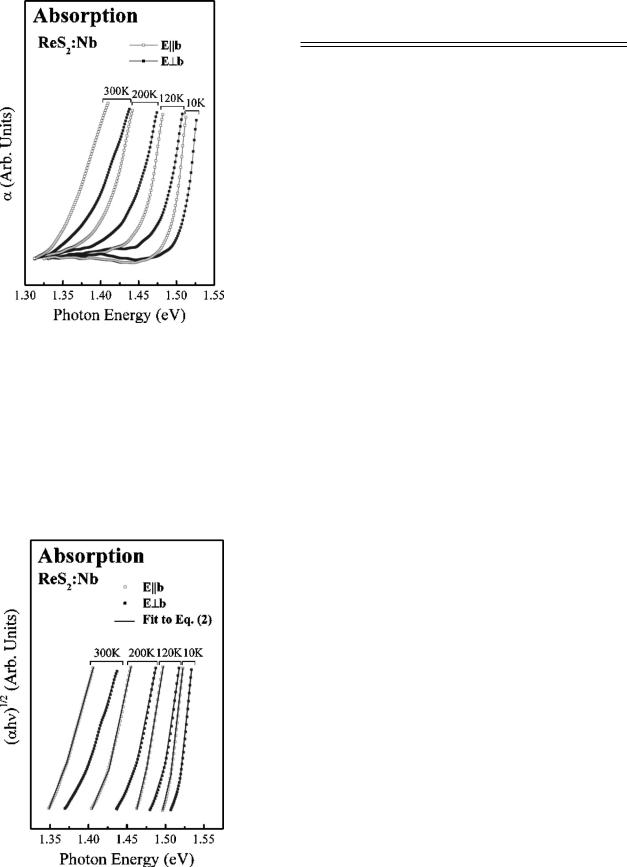
where Tr represents the transmission coefÞcient, R is the reßectivity, and d is the sample thickness. The variation of the absorption coefÞcient of ReS2 :Nb with photon energy at several representative temperatures between 10 and 300 K is presented in Fig. 2. The open-square curve corresponds to the E b polarization and the solid-square curve represents E b polarization for ReS2 :Nb. The small oscillations below the absorption edge attributed to interference effects are frequently observed for thin layered crystals.30 The polarization dependence of the absorption curves provides conclusive evidence that the two optical absorption edges are associated with interband transitions from different origins. The polarization-dependent experimental data analysis of the absorption coefÞcient shows an indirect allowed transition for the investigated materials.
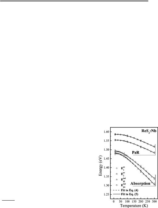
The experimental points for h 1/2 versus photon energy h deduced from polarization-dependent absorption measurements for ReS2 :Nb at several representative temperatures between 10 and 300 K are shown in Fig. 3. The open and solid squares are data points from the E b and E b polarization measurements, respectively; and the solid
curves are the least-squares Þts to the expression29 |
|
|||||
A h − Egind + Ep 2 |
|
B h − Egind − Ep 2 |
|
2 |
||
h = |
|
+ |
|
, |
||
exp Ep/kT − 1 |
1 − exp − Ep/kT |
|||||
|
|
|
|
|||
where h is the energy of the incident photon, Eindg is the indirect band gap, Ep is the energy of the phonon assisting
Downloaded 20 Oct 2007 to 219.81.17.198. Redistribution subject to AIP license or copyright, see http://jap.aip.org/jap/copyright.jsp
083523-3 |
Dumcenco et al. |
J. Appl. Phys. 102, 083523 2007 |
FIG. 2. Polarization-dependent absorption coefÞcient vs photon energy for ReS2 :Nb at several representative temperatures between 10 and 300 K. The openand solid-square curves are deduced from the transmittance spectra of E b and E b polarizations, respectively.
the transitions, and A and B are constants. The Þrst term on the right-hand side of Eq. 2 corresponds to absorption of a photon and a phonon, whereas the second term corresponds to absorption of a photon and emission of a phonon and
contributes only when h Eindg +Ep. To evaluate the band gap Eindg and phonon energy Ep with the use of Eq. 2 , the
background absorption is subtracted out. The results indicate
FIG. 3. Experimental points for h 1/2 vs h that are deduced from polarization-dependent absorption measurements for ReS2 :Nb at several representative temperatures between 10 and 300 K. The openand solidsquares are data points from the E b and E b polarization measurements, respectively, and the solid curves are the least-squares Þts to Eq. 2 .
TABLE I. The summary of the indirect band gap energies and phonon energies obtained by polarization-dependent transmittance measurements for ReS2 :Nb, ReS2 :Mo, and undoped ReS2.
|
|
|
|
Energy gap |
Phonon energy |
|
Materials |
Polarization |
Egind eV |
Ep meV |
|
|
|
|
|
|
|
ReS2 |
:Nba |
E b |
1.32±0.02 |
32±5 |
|
|
|
|
E b |
1.35±0.02 |
27±5 |
ReS2 |
:Mob |
E b |
1.31±0.02 |
32±5 |
|
|
|
|
E b |
1.33±0.02 |
23±5 |
ReS2c |
E b |
1.35±0.02 |
25±5 |
||
|
|
|
E b |
1.38±0.02 |
25±5 |
|
|
|
|
||
|
|
|
|
|
|
aThis work. |
|
|
|
||
bReference 23. cReference 17.
that the Nb-doped sample is an indirect semiconductor, in which polarization along the Re chains exhibits a smaller band gap and a single phonon makes an important contribution in assisting the indirect transitions. The nonuniform thickness and nonsmooth sample surface will tend to cause the angles of incidence to deviate from the normal direction, resulting in some variations in the absorption spectra. The indirect gaps denoted as Eindg and Eindg refer, respectively, to the indirect gap with E b and E b polarizations. Differing values of Eindg and Ep could be obtained by Þtting a different
energy range; thus, errors of the order of ±0.02 eV and ±5 meV can be deduced for the estimates of Eindg and Ep,
respectively. The Þtted values of the energy gaps and phonon energy of the ReS2 :Nb crystals at room temperature are summarized in Table I. The results show that incorporation of small amounts of niobium into ReS2 shifts the absorption edge by about 0.03 eV towards the lower energy region. This observation agreed well with the previous absorption study of Mo-doped ReS2 single crystals.23 The physical origin of the shift may come from the existence of n-type impurity, which in general will contribute to the absorption near the band tail. The parameters that describe the temperature dependence of the absorption edges with different polarizations in the van der Waals plane will be discussed in a latter section.
The typical unpolarized and polarization-dependent PL spectra of ReS2 :Nb in the 1.5Ð1.75 eV energy range at a
constant |
laser excitation intensity of 3 W/cm2 |
=532 nm |
are illustrated in Fig. 4. Unpolarized PL spectra |
and the spectra with polarization perpendicular and parallel to the chains are shown by open-triangle, open-square, and open-circle curves, respectively. To assign simple radiative bands from the complex spectrum of photoluminescence, a multipeak Lorentzian line shape analysis offered by the software ORIGIN was employed. From the line shape Þt, two well-resolved excitonic features marked by Eex1 and Eex2 at 1.552 and 1.585 eV with full width at half maximumFWHM of 13.8 and 14.6 meV, respectively, were observed in the PL spectra at 10 K. In addition, on the higher energy side of the spectra, another two peaks labeled as Eex3 and Eex4 appeared at energies of 1.631 and 1.645 eV, respectively. The two features located at the high energy side are
Downloaded 20 Oct 2007 to 219.81.17.198. Redistribution subject to AIP license or copyright, see http://jap.aip.org/jap/copyright.jsp

083523-4 |
Dumcenco et al. |
J. Appl. Phys. 102, 083523 2007 |
FIG. 4. The polarization-dependent PL spectra of ReS2 :Nb at 10 K. The Þgure shows the unpolarized open triangles , and polarized perpendicularopen squares and along open circles to b-axis PL spectra.
barely resolved with an energy separation of 14 meV, while the well-resolved features Eex1 and Eex2 have an energy difference of 33 meV. As shown in Fig. 4, the Eex1 excitonic peak is forbidden for E b polarization, whereas the Eex2 peak is disallowed for E b polarization. Our experiments indicated that the two PL peaks Eex3 and Eex4 have shown no polarization dependency as both features were observed in E b and E b polarization spectra. It is also worth noting that the intensities of Eex3 and Eex4 for the Nb-doped sample are signiÞcantly enhanced by comparing with the undoped and Mo-doped ReS2. The entirely different polarization selection rules for these four features show that they originated from totally different origins. Temperaturedependent PL spectra of the excitonic transitions in the temperature range between 10 and 90 K are demonstrated in Fig. 5. The open triangles are the experimental data of unpolarized PL spectra and the solid lines are least-square Þts to the multipeak Lorentzian line shape that yield transition energies indicated by arrows. As the temperature increases, the excitonic features demonstrate an energy redshift behavior as well as the decreasing character of line intensities. The intensities of Eex3 and Eex4 features decrease rather drastically with respect to temperature increasing and become completely quenched at T=90 K.
Previous research reports concerning the optical property study of ReS2 utilizing PzR have revealed optical anisotropy consisting of strong polarization dependence of interband excitonic transitions in the vicinity of the direct band gap Edg.12,31 The temperature-dependent PzR spectra of ReS2 :Nb with E b and E b polarizations at various temperatures between 10 and 300 K are shown in Fig. 6. The open-circle and open-square curves are, respectively, the experimental PzR spectra of E b and E b polarizations. In the low energy side of PzR spectra, two dominant structures associated with band-edge excitonic transitions were identiÞed: the Eex1 feature was detected at E b polarization while Eex2 feature was observed at E b polarization only.12,17 The higher ly-
FIG. 5. Temperature-dependent unpolarized PL spectra of ReS2 :Nb in the temperature range between 10 and 90 K. The open triangles are the experimental data and the solid curves are the least-squares Þts.
ing Eex3 and Eex4 features were also detected. It should be mentioned that intensity of PzR signal at the higher energy region is quite similar to the PL counterparts, showing considerable enhancement for Nb-doped ReS2 in comparing with the previous investigations of undoped and Mo-doped ReS2 single crystals.12
FIG. 6. Temperature-dependent PzR spectra of ReS2 :Nb at several temperatures between 10 and 300 K. The open circles and open squares correspond to the experimental data of E b and E b polarizations, respectively, and the solid curves are least-squares Þts to Eq. 3 .
Downloaded 20 Oct 2007 to 219.81.17.198. Redistribution subject to AIP license or copyright, see http://jap.aip.org/jap/copyright.jsp
083523-5 |
Dumcenco et al. |
|
|
|
|
|
J. Appl. Phys. 102, 083523 2007 |
|||
|
|
TABLE II. The summary of the energy positions and broadening parameters of the near band-edge excitonic |
||||||||
|
|
transitions determined by polarization-dependent PzR measurements |
for ReS2 :Nb. |
Previous results of |
||||||
|
|
ReS2 |
:Mo and undoped ReS2 are listed for comparison. |
|
|
|
|
|
||
|
|
|
|
|
|
|
|
|
||
|
|
|
|
|
|
|
|
|
||
|
|
|
|
|
Excitonic transition energy eV |
|
Broadening parameter meV |
|||
|
|
|
|
|
|
|
|
|
|
|
|
|
Material |
Temperature K |
E1ex |
E2ex |
|
1ex |
2ex |
||
|
|
|
|
|
|
|
|
|
|
|
|
|
ReS2 |
:Nba |
20 |
1.555±0.001 |
1.588±0.001 |
7±1 |
7±1 |
|
|
|
|
|
|
300 |
1.485±0.002 |
1.519±0.002 |
32±2 |
22±2 |
|
|
|
|
ReS2 |
:Mob |
30 |
1.554±0.001 |
1.585±0.001 |
8±1 |
7±1 |
|
|
|
|
|
|
300 |
1.485±0.002 |
1.516±0.002 |
35±2 |
23±2 |
|
|
|
|
ReS2b |
30 |
1.554±0.001 |
1.584±0.001 |
6±1 |
6±1 |
|
||
|
|
|
|
300 |
1.484±0.002 |
1.518±0.002 |
31±2 |
21±2 |
|
|
aThis work. bReference 23.
In order to determine the energy positions associated with observed optical transitions and to identify those unknown spectral features, the PzR spectrum of excitonic transitions has been Þtted by a Lorentzian line shape expression,32
|
R |
|
n |
|
|
|
|
|
|
= Re |
Aiexej iex E − Eiex + j iex −2 |
, |
3 |
||||
|
||||||||
|
R |
i=1 |
|
|
|
|||
where Aex and ex |
are the amplitude and phase of the line |
|||||||
|
|
i |
i |
|
|
|
|
|
shape, and Eexi and exi are the energy and broadening parameters of the interband excitonic transitions, respectively. The Þtting results illustrated as solid lines Fig. 6 are the leastsquares Þts to the experimental data. Arrows at the bottom of PzR spectra show the peak positions of the main excitonic features, respectively. The values of transition energies and broadening parameters at room temperature and 10 K, analyzed by Eq. 3 , are presented in Table II. The parameters of the near band-edge excitonic transitions determined by polarization-dependent PzR measurements of Mo-doped ReS2 Ref. 23 and undoped ReS2 Ref. 23 are listed in Table II for comparison purpose. The Þtting results of ReS2 :Nb samples conÞrm that the direct band-edge excitonic transition energies Eex1 and Eex2 are not sensitive to a small concentration of niobium doping, and broadening parameter values are slightly increased due to impurity scattering. These observations agree with the results reported previously for Moand W-doped ReSe2 single crystals.24 The values of transition energies obtained in the PzR spectra are consistent with those of the PL spectra.
The experimental values of the temperature dependence of Eex1 T and Eex2 T as well as Eindg T and Egind T for ReS2 :Nb are presented in Fig. 7. The uncertainties of experi-
mental data are expressed in the form of representative error bars. The dotted curves in Fig. 7 are the least-squares Þt to
the Varshni empirical relationship,33 |
|
iT2 |
|
Ei T = Ei 0 − i + T , |
4 |
and i obtained for excitonic transitions in ReS2 :Nb are listed in Table III. For comparison purposes, the numbers for undoped ReS2 determined from PzR,12 thermoreßectanceTR ,20 and photorefelctance22 PR are also listed in Table III.
The temperature-dependent data of the interband excitonic transition energies have also been Þtted by an expres-
sion containing the Bose-Einstein occupation factor for phonon,34,35
2 |
|
|
|
Ei T = EiB − aiB 1 + |
|
, |
5 |
exp iB/T − 1 |
|||
where i=1 or 2, aiB represents the strength of the electronexciton -phonon interaction, and iB corresponds to the average phonon temperature. The Þtted results are shown in Fig. 7 by solid lines. The obtained values of EiB, aiB, and iB for ReS2 :Nb, and the corresponding values for undoped ReS2 determined from PzR Ref. 12 and TR Ref. 20 are given in Table III for comparison.
where i=1 or 2, Ei 0 is the transition energy at 0 K, and i and i are Varshni coefÞcients. The constant i is related to the electron exciton -phonon interaction and i is closely related to the Debye temperature. The values of Ei 0 , i,
FIG. 7. The temperature dependence of the polarization-dependent excitonic transition energies and indirect band gaps of ReS2 :Nb with representative error bars. The dashed curves are the least-squares Þts to Eq. 4 and the solid lines are Þtted to Eq. 5 .
Downloaded 20 Oct 2007 to 219.81.17.198. Redistribution subject to AIP license or copyright, see http://jap.aip.org/jap/copyright.jsp

083523-6 |
Dumcenco et al. |
J. Appl. Phys. 102, 083523 2007 |
TABLE III. The values of the Þtting parameters of Varshni equation and an expression containing the BoseEinstein occupation factor for phonon which describe the temperature dependence of polarization-dependent band-edge excitonic transition energies, and indirect band gaps determined from absorption Abs measurements of ReS2 :Nb and undoped ReS2. The results obtained by TR and PR are also included for comparison.
|
|
E 0 |
|
|
EB |
aB |
B |
||
Materials |
Feature |
eV |
meV/K |
K |
eV |
meV |
K |
||
|
|
|
|
|
|
|
|
|
|
ReS2 :Nb PzR a |
E1ex |
1.556± |
0.005 |
0.40±0.05 |
195±70 |
1.588± |
0.005 |
33±10 |
200±50 |
|
Eex |
1.589± |
0.005 |
0.39±0.05 |
195±70 |
1.619± |
0.005 |
32±10 |
200±50 |
|
2 |
|
|
|
|
|
|
|
|
ReS2 PzR b |
E1ex |
1.554± |
0.005 |
0.36±0.05 |
175±75 |
1.583± |
0.008 |
32±10 |
200±50 |
|
Eex |
1.588± |
0.005 |
0.37±0.05 |
175±75 |
1.619± |
0.008 |
34±10 |
200±50 |
|
2 |
|
|
|
|
|
|
|
|
ReS2 TR c |
E1ex |
1.546± |
0.001 |
0.34±0.05 |
180±70 |
1.584± |
0.002 |
37±15 |
240±60 |
|
Eex |
1.577± |
0.001 |
0.33±0.05 |
190±70 |
1.613± |
0.002 |
35±14 |
240±60 |
|
2 |
|
|
|
|
|
|
|
|
ReS2 PR d |
E1ex |
1.558± |
0.005 |
0.37±0.05 |
175±75 |
|
|
|
|
|
Eex |
1.591± |
0.005 |
0.35±0.05 |
180±75 |
|
|
|
|
|
2 |
|
|
|
|
|
|
|
|
ReS2:Nb Abs a |
Egind |
1.48± |
0.02 |
0.86±0.05 |
130±50 |
1.55± |
0.02 |
70±20 |
180±50 |
|
Eind |
1.50± |
0.02 |
0.75±0.05 |
130±50 |
1.55± |
0.02 |
60±20 |
180±50 |
|
g |
|
|
|
|
|
|
|
|
ReS2 Abs e |
Egind |
1.51± |
0.02 |
0.73±0.05 |
133±50 |
1.57± |
0.02 |
66±21 |
194±50 |
|
Eind |
1.52± |
0.02 |
0.68±0.05 |
128±50 |
1.58± |
0.02 |
62±18 |
193±50 |
|
g |
|
|
|
|
|
|
|
|
aThis work. bReference 12. cReference 20. dReference 22. eReference 15.
As shown in Table III, the values of the electron-phonon coupling constants i in Eq. 4 and aiB in Eq. 5 , which describe the temperature dependence of the indirect band gaps for ReS2, are larger than those for the direct band-edge excitonic transition energies. The phenomena can be explained by the fact that the reduction in the thermal broadening of the exciton causes a faster shift of the absorption tail with temperature lowering. These results are similar to the previous reports on low energy absorption in MoS2 and MoSe2 layered crystals.36
The experimental values of the linewidth exi T of ReS2 :Nb as obtained from the line shape Þt are displayed in Fig. 8 by the solid open circles and open squares with representative error bars for the Eex1 and Eex2 excitonic transitions, respectively. The temperature dependence of the linewidth can be expressed as34,35
iLO |
|
|
i T = i0 + exp iLO/T − 1 |
, |
6 |
where i=1 or 2. The Þrst term represents the broadening invoked from temperature-independent mechanisms, such as impurity, dislocation, electron interaction, and Auger processes, while the second term is caused by the Fršhlich interaction. The quantity iLO represents the strength of the electron exciton -LO phonon coupling while iLO is the LO phonon temperature. The solid curves in Fig. 8 represent least-squares Þts of the experimental data which enable the evaluation of i0, iLO, and iLO for the excitonic transitions of ReS2 :Nb. The obtained values of these quantities are listed in Table IV together with the numbers for undoped ReS2 determined by PzR Ref. 12 and TR measurements.20
For comparison purposes, the numbers for Þtting parameters from previous reports on polarization-dependent transi-
tion energies determination of undoped ReS2 single crystals, measured by PzR,12 TR,20 and PR,22 are also included. As shown in Table III, the values of Varshni coefÞcients i andi, and at the same time parameters of expression containing Bose-Einstein occupation factor aiB and iB determined by PzR measurements of ReS2 :Nb, are in good agreement with previous Þtting results of undoped ReS2.12 The i values for both Eex1 and Eex2 excitonic transitions equal to 195±70 K for ReS2 :Nb are in reasonable agreement with Debye temperature estimated from the LindemannÕs formula for undoped ReS2.12 The high-temperature limits of Eqs. 4 and 5 yield
FIG. 8. The temperature dependence of the polarization-dependent linewidth of excitonic transitions of ReS2 :Nb with representative error bars. The solid curves are the least-squares Þts to Eq. 6 .
Downloaded 20 Oct 2007 to 219.81.17.198. Redistribution subject to AIP license or copyright, see http://jap.aip.org/jap/copyright.jsp

083523-7 Dumcenco et al.
TABLE IV. The values of the parameters which describe the temperature dependence of the broadening function of the band-edge excitonic transitions of ReS2 :Nb and undoped ReS2.
|
|
0 |
LO |
LO |
Materials |
Feature |
meV |
meV |
K |
|
|
|
|
|
ReS2 :Nba |
E1ex |
6.9±1.0 |
57±15 |
350±100 |
|
Eex |
7.1±1.0 |
42±15 |
350±100 |
|
2 |
|
|
|
ReS2 PzR b |
E1ex |
5.5±1.0 |
74±28 |
395±100 |
|
Eex |
7.8±1.0 |
42±8 |
363±50 |
|
2 |
|
|
|
ReS2 TR c |
E1ex |
9.5±0.5 |
36±15 |
326±100 |
|
Eex |
8.0±0.5 |
30±17 |
348±100 |
|
2 |
|
|
|
|
|
|
|
|
aThis work. |
|
|
|
|
bReference 12. |
|
|
|
|
cReference 20. |
|
|
|
|
an expression i 2aiB / iB |
which is satisÞed within error |
|||
bars for the obtained parameters i, aiB, and iB of Table III. The temperature variations of excitonic-transition energies are due to both the lattice-constant variations and interactions with relevant acoustic and optical phonons. According to the existing theory, this should lead to a value of iB signiÞcantly smaller than iLO and agree favorably with our present experimental investigations.
The values of the parameters which describe the temperature dependence of broadening function of the excitonic transitions of ReS2 :Nb are comparable to those of undoped
ReS2. The values for the coupling constant 1LO and 2LO for ReS2 :Nb are in the range of 40Ð60 meV, which are consid-
erably larger than those reported for a number of semiconductors, such as GaAs 20 meV Ref. 37 and ZnSe24 meV .38 We suspected that the large values of LO may be the general characteristics of crystals with layer structure. However, a more systematic experimentation should be carried out to verify this property.
IV. SUMMARY
The effects of Nb dopant on the optical properties were studied. The results indicate that incorporation of niobium into the host lattice ReS2 can cause a small redshift of the indirect energy gap of the Nb-doped ReS2 sample as determined from the transmittance spectra. The PL spectra of ReS2 :Nb observed by means of linearly polarized light at normal incidence to the basal plane revealed two strongly polarization-dependent main peaks, Eex1 and Eex2 , while the higher lying Eex3 and Eex4 peaks have shown no polarization dependence. The direct band-edge excitonic transition energies Eex1 and Eex2 of ReS2 :Nb single crystals obtained by PzR measurements remain practically unchanged in comparison with undoped ReS2. Nevertheless, the doping effect shows up in a slight increase of the broadening parameter of the excitonic features. It is also worth noting that, by doping with niobium, the intensities of the higher lying Eex3 and Eex4 peaks have signiÞcantly enhanced over that of the samples doped with Mo.
J. Appl. Phys. 102, 083523 2007
ACKNOWLEDGMENT
The authors would like to acknowledge the Þnancial support by the National Science Council of Taiwan under Grant Nos. NSC95-2112-M-011-001, NSC95-2221-E-011- 171, and NSC 95-2112-M-019-001.
1J. A. Wilson, F. J. DiSalvo, and S. Mahajan, Adv. Phys. 24, 117 1975 . 2J. C. Wildervanck and F. Jellinek, J. Less-Common Met. 24, 73 1971 . 3J. A. Wilson and A. D. Yoffe, Adv. Phys. 18, 193 1969 .
4G. Leicht, H. Berger, and F. Levy, Solid State Commun. 61, 531 1987 . 5K. Friemelt, O. Kulikova, L. Kulyuk, A. Siminel, E. Arushanov, Ch. Kloc, and E. Bucher, J. Appl. Phys. 79, 9268 1996 .
6H. S. Broadbent, L. H. Slaugh, and N. L. Jarvis, J. Am. Chem. Soc. 76, 1519 1954 .
7S. Harris and R. R. Chianelli, J. Catal. 86, 400 1984 .
8F. P. Koffyberg, K. Dwight, and A. Wold, Solid State Commun. 30, 4331979 .
9B. L. Wheeler, J. K. Leland, and A. J. Bard, J. Electrochem. Soc. 133, 3581986 .
10J. V. Marzik, R. Kershaw, K. Dwight, and A. Wold, J. Solid State Chem. 51, 170 1984 .
11B. Schubert and H. Tributsch, J. Appl. Electrochem. 20, 786 1990 . 12C. H. Ho, P. C. Liao, Y. S. Huang, and K. K. Tiong, Phys. Rev. B 55,
15608 1997 .
13K. K. Tiong, C. H. Ho, and Y. S. Huang, Solid State Commun. 111, 6351999 .
14C. H. Ho, Y. S. Huang, P. C. Liao, and K. K. Tiong, J. Phys. Chem. Solids
60, 1797 1999 .
15C. H. Ho, Y. S. Huang, K. K. Tiong, and P. C. Liao, Phys. Rev. B 58,
16130 1998 .
16C. H. Ho, Y. S. Huang, J. L. Chen, T. E. Dann, and K. K. Tiong, Phys. Rev. B 60, 15766 1999 .
17C. H. Ho, Y. S. Huang, K. K. Tiong, and P. C. Liao, J. Phys.: Condens. Matter 11, 5367 1999 .
18C. H. Ho, P. C. Yen, Y. S. Huang, and K. K. Tiong, J. Phys.: Condens. Matter 13, 8145 2001 .
19C. H. Ho, H. W. Lee, and C. C. Wu, J. Phys.: Condens. Matter 16, 59372004 .
20C. H. Ho, Opt. Express 13, 8 2004 .
21K. Friemelt, M.-Ch. Lux-Steiner, and E. Bucher, J. Appl. Phys. 74, 5266
1993 .
22C. H. Ho, P. C. Yen, Y. S. Huang, and K. K. Tiong, Phys. Rev. B 66,
245207 2002 .
23P. C. Yen, M. J. Chen, Y. S. Huang, C. H. Ho, and K. K. Tiong, J. Phys.:
Condens. Matter 14, 4737 2002 .
24S. Y. Hu, S. C. Lin, K. K. Tiong, P. C. Yen, Y. S. Huang, C. H. Ho, and P.
C. Liao, J. Alloys Compd. 383, 63 2004 .
25S. Y. Hu, C. H. Liang, K. K. Tiong, Y. S. Huang, and Y. C. Lee, J.
Electrochem. Soc. 153, J100 2006 .
26Y. S. Huang, Chin. J. Phys. Taipei 22, 43 1984 .
27F. H. Pollak and H. Shen, Mater. Sci. Eng., R. 10, 275 1993 . 28H. Mathieu, J. Allegre, and B. Gil, Phys. Rev. B 43, 2218 1991 .
29J. I. Pankove, Optical Processes in Semiconductors Dover, New York,
1975 .
30K. K. Kam, C. L. Chang, and D. W. Lynch, J. Phys. C 17, 4031 1984 . 31C. H. Ho, P. C. Liao, Y. S. Huang, and K. K. Tiong, Solid State Commun.
103, 19 1997 .
32D. E. Aspnes, in Handbook on Semiconductors, edited by M. BalkanskiNorth-Holland, Amsterdam, 1980 , p. 109.
33Y. P. Varshni, Physica Amsterdam 34, 149 1967 .
34P. Lantenschlager, M. Garriga, S. Logothetidis, and M. Cardona, Phys. Rev. B 35, 9174 1987 .
35P. Lantenschlager, M. Garriga, L. Vina, and M. Cardona, Phys. Rev. B 36, 4821 1987 .
36A. M. Goldberg, A. R. Beal, F. A. Levy, and E. A. Davis, Philos. Mag. 32, 367 1975 .
37H. Qiang, F. H. Pollak, C. M. Sotomayer Torres, W. Leitch, A. H. Kean, M. Stroscio, G. J. Jafrate, and K. W. Kim, Appl. Phys. Lett. 61, 14111992 .
38L. Malikova, W. Krystek, F. H. Pollak, N. Dai, A. Cavus, and M. C. Tamargo, Phys. Rev. B 54, 1819 1996 .
Downloaded 20 Oct 2007 to 219.81.17.198. Redistribution subject to AIP license or copyright, see http://jap.aip.org/jap/copyright.jsp
INSTITUTE OF PHYSICS PUBLISHING |
JOURNAL OF PHYSICS: CONDENSED MATTER |
|
|
J. Phys.: Condens. Matter 15 (2003) 1487–1494 |
PII: S0953-8984(03)55681-8 |
The first-order Raman spectra of OsO2
P C Yen1, R S Chen1, Y S Huang1,4, C T Chia2, R H Chen2 and
K K Tiong3
1Department of Electronic Engineering, National Taiwan University of Science and Technology, Taipei 106, Taiwan, Republic of China
2Department of Physics, National Taiwan Normal University, Taipei 117, Taiwan,
Republic of China
3 Department of Electrical Engineering, National Taiwan Ocean University, Keelung 202, Taiwan, Republic of China
Received 6 November 2002, in final form 22 January 2003
Published 24 February 2003
Online at stacks.iop.org/JPhysCM/15/1487
Abstract
The first-order Raman spectra of the transition metal dioxide OsO2 with tetragonal rutile structure have been measured at room temperature. A linearly polarized argon laser light source and completely oriented single-crystal samples have made possible unambiguous determination of the four allowed Raman-active phonon modes. Comparison is made with results for other rutile materials.
1. Introduction
The family of transition metal dioxide compounds with rutile-type structure possesses an interesting variety of electrical and magnetic properties [1]. Conductive transition metal dioxides with rutile-type structure show potential applications in substituting for the metals currently used in conductive lines which serve to connect components of semiconductor and electrode materials in ferroelectric memory devices [2–4]. Osmium dioxide, OsO2, belongs to this family of compounds; little is known of its fundamental properties. This may be due in part to the highly toxic nature of the readily formed and volatile tetroxide of the material [5].
This report presents the first-order Raman spectra of OsO2. To the best of our knowledge only one such report on the phonon frequencies of the four Raman-active modes in OsO2 exists [6]. The existing literature merely lists a Raman spectrum from a small crystal of OsO2, oriented so as to display all four Raman-active lines. In the present study, the group symmetry restraints of the Raman-active phonons and the Raman selection rules are discussed. The results are then utilized to classify the experimentally observed polarized Raman spectra of the four phonon modes. Comparisons are made with results for other metal dioxide [7–13] and metal fluoride [10, 14] compounds, which possess similar rutile-type structure.
4 Author to whom any correspondence should be addressed.
0953-8984/03/091487+08$30.00 © 2003 IOP Publishing Ltd Printed in the UK |
1487 |
1488 |
P C Yen et al |
Figure 1. A photograph of an OsO2 crystal showing the (110) and (111) planes together with the polarization axes.
2. Experimental details
Single crystals of OsO2 with well-developed faces were grown in our laboratory by the chemical transport method [15]. OsO2 was grown by the oxidation of high-purity osmium with excess NaClO3 or NaBrO3 in an evacuated, sealed silica tube. The volume of the tube was about 100 cm3 after sealing, and the excess NaClO3 or NaBrO3 was sufficient to complete oxidation of Os to OsO2. The processes of NaClO3 or NaBrO3 decomposition and Os oxidation were accomplished simultaneously by slowly heating the silica tube and its contents to 300 ◦C over 48 h and subsequently firing at 650 ◦C for an additional 48 h. This treatment resulted in an apparent complete decomposition of the chlorate or bromate with the formation of golden OsO2 powder in one end of the tube. The tube was then transferred to a horizontal furnace and positioned so as to provide a temperature gradient along the length of the tube, which is about 20 cm long. The charge of OsO2 in one end was maintained at 920 ◦C, and the opposite end of the tube was held at 900 ◦C for 240 h. The transported crystals were about 3–5 mm across a polyhedral face. The x-ray powder diffraction analysis was performed to ascertain that tetragonal rutile structure had been obtained. The crystals were x-ray pre-oriented with respect to the directions and polarizations of the incident and scattered light. A representative crystal showing the as-grown (110) and (111) planes together with the prescribed polarization configurations is illustrated in figure 1.
Raman measurements were made on as-grown (110) and (111) faces in the backscattering geometry utilizing a DILOR XY-800 triple-grating Raman spectrometer equipped with a liquid- nitrogen-cooled CCD and an OLYMPUS BH-2 microscope. The 5145 Å line of an argon ion laser was used as the excitation source, and was focused on the sample surface with a 100× objective. The focusing spot size is about 1 µm in diameter and the laser power density is estimated to be about 1 W cm−2. Prior to the measurement,the system was calibrated by means of the 520 cm−1 Raman peak of a Si single crystal. The spectra exhibited approximately a 0.5 cm−1 resolution with the slit width of 30 µm. For frequency less than 250 cm−1, an argon purge was used to suppress the N2 lines.
3. Symmetry analysis
OsO2 has the tetragonal rutile structure belonging to the space group D144h with two OsO2 molecules per unit cell as shown in figure 2. The cations are located at sites with D2h symmetry