

-
As a result of multiplying the 2-machine numbers with n-bit mantissa in the result register
~Always become 0
~Always become 1
=Possible loss of normalization
~Always normalized number
~No right answer
-
As shown in Fig. connection of transistors (circuit) implements the logic function

~Negation(NOT)
~Conjunction
=Negative conjunction(NAND)
~Negative disjunction(NOR)
~Disjunction
-
As shown in Fig. Two compound transistors (circuit) implements the logic function

~conjunction
~disjunction
=negative disjunction(NOR)
~negative conjunction(NAND)
~negation(NOT)
-
Decoder is a chip containing n binary inputs and how many outputs?
=2n outputs
~2 + n outputs
~n2 outputs
~n + 2 outputs
~No right answer
-
During the conversion of the virtual address, when does the lookup of the TLB in buffer take place?
=The lookup always precedes the pages' tables lookup
~The lookup sometimes precedes the pages' tables lookup
~The lookup replaces the cache search
~The lookup doesn't hold any place
~No right answer
-
For performing the addition and subtraction operations of two n-order numbers, the common scheme consisting of n blocks accompanied with the XOR chip with one output (γ1) as a decoder connection is used. What is the γ1 value of the operating signal for the addition operation?
~1
=0
~2
~3
~No right answer
-
For performing the addition and subtraction operations of two n-order numbers, the common scheme consisting of n blocks accompanied with the XOR chip with one output (γ1) as a decoder connection is used. In case of addition of two positive numbers the chip transforms the negative summand into the additional code. For which γ1 value the chip does so?
~Equal 1
~Equal 0
~Equal 2
~Equal 3
=No right answer
-
For performing the addition and subtraction operations of two n-order numbers, the common scheme consisting of n blocks accompanied with the XOR chip with one output (γ1) as a decoder connection is used. In case of subtraction the chip transforms the negative summand onto the additional code. For which γ1 value the chip does so?
=Equal 1
~Equal 0
~Equal 2
~Equal 3
~No right answer
-
How many transistors do you usually need for disjunction?
=3
~2
~1
~5
~No right answer
-
How much information does one RS-trigger chip store?
=1-n bit
~1-n byte
~Machine word
~Double word
~No right answer
-
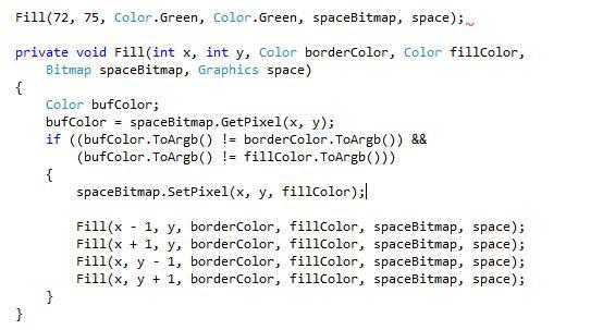
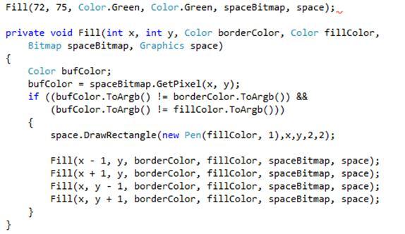
How this algorithm does fill the shape?

~draws the line to the left edge of the shape
~draws the line from edge to edge a shape
=fills only the upper part of the shape
~fills the entire shape
~No right answer.
-
How this algorithm does fill the shape?

~draws the line to the left edge of the shape
=draws the line from edge to edge a shape
~fills only the upper part of the shape
~fills the entire shape
~No right answer.
-
How this algorithm does fill the shape?

=draws the line to the left edge of the shape
~draws the line from edge to edge a shape
~fills only the upper part of the shape
~fills the entire shape
~No right answer.
-
How this algorithm does fill the shape?
~draws the line to the left edge of the shape
~draws the line from edge to edge a shape
~fills only the upper part of the shape
=fills the entire shape
~No right answer.
-
If during the execution of the program is necessary to the operation of division in which the divider takes the value "0", then the resulting system
~Returns 1 as result
~Returns 0 as result
=Returns special message, and interrupts program
~Nothing occurs
~No right answer
-
If m base of the system and 2 ±


 is floating point number. What is the maximum number that can be
represented?
is floating point number. What is the maximum number that can be
represented?
=
![]()
~m <sup>k</sup> - 1
~![]()
~1-m<sup>- n</sup>
~No right answer
-
If we assume one-digit adder circuit in Fig. a separate unit, how many of these units will be required to implement the addition of 2 binary vectors of length n
~n/2#
=2<sup>n</sup>#
=n#
~n<sup>2</sup>#
~no right answer#
-
In addition to minuend, subtrahend's orders what does the difference result for the for the single-order adder-subtractor chip performing subtraction operation consider?
~Transfer during addition
~Overflow
~Division by zero symptom
=Lease value of the give order
~No right answer
-
In multiplexer 8x1 what control bits we have to configure to get information from 1st pin
~001
~011
=000
~101
~111
-
In multiplexer 8x1 what control bits we have to configure to get information from 2nd pin
~000
~011
=001
~101
~111
-
In multiplexer 8x1 what control bits we have to configure to get information from 3rd pin
~000
~011
=010
~101
~111
-
In multiplexer 8x1 what control bits we have to configure to get information from 4th pin
~001
~010
=011
~101
~111
-
In multiplexer 8x1 what control bits we have to configure to get information from 5th pin
~000
~011
=100
~101
~111
-
In multiplexer 8x1 what control bits we have to configure to get information from 6th pin
~000
~011
=101
~110
~111
-
In multiplexer 8x1 what control bits we have to configure to get information from 7th pin
~000
~011
=110
~101
~111
-
In multiplexer 8x1 what control bits we have to configure to get information from 8th pin
~000
~011
=111
~110
~101
-
It is known that to achieve the logical function "disjunction" is required
~One transistor
~Two transistors
=Three transistors
~Four transistors
~no right answer
-
It is known that to achieve the logical function "negation of the conjunction" (NAND) is required
~One transistor
~Three transistors
=Two transistors
~Four transistors
~no right answer
-
It is known that to achieve the logical function "negation of the disjunction" (NOR) is required
~One transistor
~Three transistors
=Two transistors
~Four transistors
~no right answer
-
Let
 be a floating point number and let n be the size of mantissa and k
the size of the cells.
be a floating point number and let n be the size of mantissa and k
the size of the cells.
What is the minimum normalized number that is not
equals to zero such as
![]()
=
![]()
~![]()
~![]()
~
~![]()
-
Let
 be a floating point number with the base 2 and let n be the size of
mantissa and k the total amount of cells. What is the minimum
normalized number that is not equals to zero?
be a floating point number with the base 2 and let n be the size of
mantissa and k the total amount of cells. What is the minimum
normalized number that is not equals to zero?
=
![]()
~![]()
~![]()
~![]()
~No right answer
-
Let
 be a floating point number with the base 2 and let n be the size of
mantissa and k the total amount of cells. What is the minimum NOT
normalized number that is not equals to zero?
be a floating point number with the base 2 and let n be the size of
mantissa and k the total amount of cells. What is the minimum NOT
normalized number that is not equals to zero?
=
![]()
~![]()
~![]()
~![]()
~No right answer
-
Let ±


 be a machine number with k cell size n mantissa. What is the
maximum number that can be represented?
be a machine number with k cell size n mantissa. What is the
maximum number that can be represented?
=
![]()
~</sup>2<sup> k
~</sup>2<sup> k-1
~</sup>2<sup> k</sup>+1
~No right answer
-
Let m=10, n=3, where n size of mantissa. For the number x that is equal to 0,317 with good precision result number can be
=10<sup>0</sup><sub>* </sub>0, 3171
~10<sup>0</sup><sub>* </sub>0, 3172
~10<sup>0</sup><sub>* </sub>0, 315
~10<sup>0</sup><sub>* </sub>0, 319
~10<sup>0</sup><sub>* </sub>0, 318
-
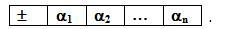
Let the base of the system be m = 2.Let we have n length cell. We are putting dot on the right of the LSB (Least Significant Bit) cell and checking number with fixed point. MSB (Most Significant Bit) will be responsible for the minus or plus sign. What is the maximum number that can be stored in given cell?

~If we will write α1=2, α2=1 , ... αn=0 in all remained positions
~If we will write α<sub>i</sub>\=3, where i\=1,2,...,n in all remained positions
=If we will write αi=1, where i=1,2,...,n in all remained positions
~If we will write α<sub>1</sub>\=1, α<sub>2</sub>\=0, ... α<sub>n</sub>\=0 in all remained positions
~No right answer
-
Let the base of the system be m = 2.Let we have n length cell. We are putting dot on the right of the LSB(Least Significant Bit) cell and checking number with fixed point. MSB (Most Significant Bit) will be responsible for the minus or plus sign. What is the maximum number that can be stored in given cell?

~10<sup>2</sup>-1
~3<sup>n</sup>-1
=2n-1
~n<sup>2</sup>-1
~No right answer
-
Let the base of the system be m = 4.Let we have n length cell. We are putting dot on the right of the LSB(Least Significant Bit) cell and checking number with fixed point. MSB (Most Significant Bit) will be responsible for the minus or plus sign. What is the maximum number that can be stored in given cell?
~If we will write α<sub>1</sub>\=3, α<sub>2</sub>\=2 , ... α<sub>n</sub>\=1 in all remained positions
~If we will write α<sub>i</sub>\=4, where i\=1,2,...,n in all remained positions
=If we will write αi=3, where i=1,2,...,n in all remained positions
~If we will write α<sub>1</sub>\=1, α<sub>2</sub>\=2, ... α<sub>n</sub>\=4 in all remained positions
~No right answer
-
Let the base of the system be m \= 8.Let we have n length cell. We are putting dot on the right of the LSB(Least Significant Bit) cell and checking number with fixed point. MSB (Most Significant Bit) will be responsible for the minus or plus sign. What is the maximum number that can be stored in given cell?

~If we will write α<sub>1</sub>\=7, α<sub>2</sub>\=6 , ... α<sub>n</sub>\=1 in all remained positions
~If we will write α<sub>i</sub>\=8, where i\=1,2,...,n in all remained positions
=If we will write αi=7, where i=1,2,...,n in all remained positions
~If we will write α<sub>1</sub>\=1, α<sub>2</sub>\=2, ... α<sub>n</sub>\=7 in all remained positions
~No right answer
-
Let the floating-point number is х= ±mp

 ,
where m is the base, p-order of ̅m - and an n-bit mantissa. We
normalized the number of x
,
where m is the base, p-order of ̅m - and an n-bit mantissa. We
normalized the number of x
~0 <\= ̅m < 1
~1/2 <\= ̅m <\= 1
=a1 !\= 0 (a1 is first bit of mantissa)
~a1<sub> </sub>\= 0
~no right answer
-
Let the integer m be the base of the system, where m = 10. What most significant digit that can be used in m based system?
~10
~7
=9
~1
~No right answer
-
Let the integer m be the base of the system, where m = 16. How many significant digits can be used to record one position in a number with such base?
~15
~17
=16
~1
~8
-
Let the integer m be the base of the system, where m = 16. What most significant digit that can be used in m based system?
~A
~0
=F
~G
~No right answer
-
Let the integer m be the base of the system, where m = 16. What symbols are used to denote m based numbers?
~1,2,3..9
~0,1,2,3..9
=0,1,2,3..9,A,B,C,D,E,F
~1,2,3..9,A,B,C,D,E,F
~No right answer
-
Let the integer m be the base of the system, where m = 2. How many significant digits can be used to record one position in a number with such base?
~3
~1
=2
~4
~0
-
Let the integer m be the base of the system, where m \= 2. What most significant digit that can be used in m based system?{
~2
~0
=1
~3
~No right answer
-
Let the integer m be the base of the system, where m = 2. What symbols are used to denote m based numbers?
~1,2
~0,2
=0,1
~1,3
~No right answer
-
Let the integer m be the base of the system, where m \= 4. How many significant digits can be used to record one position in a number with such base?{
~3
~2
=4
~1
~0
-
Let the integer m be the base of the system, where m \= 4. What most significant digit that can be used in m based system?{
~4
~2
=3
~1
~No right answer
-
Let the integer m be the base of the system, where m \= 4. What symbols are used to denote m based numbers?
~1,2,3
~0,1,2
=0,1,2,3
~0,1
~No right answer
-
Let the integer m be the base of the system, where m \= 8. How many significant digits can be used to record one position in a number with such base?{
~7
~6
=8
~5
~4
-
Let the integer m be the base of the system, where m \= 8. What most significant digit that can be used in m based system?
~8
~5
=7
~0
~No right answer
-
Let the integer m be the base of the system, where m \= 8. What symbols are used to denote m based numbers?
~1,2,3..8
~1,2,3..7
=0,1,2,3..7
~1,2,3..6
~No right answer
-
Select one of the advantages of representing integers as the code with offset.
=absence of dual representation of a "zero"
~presence of the sign (plus or minus sign in the number)
~ability to represent numbers from unlimited range
~presence of mantissa
~No right answer
-
The amount of summands in the expansion formula ⋁& according to the given function's truth table during the construction of the complete conjunctive-normal form of the given Boolean function is equal to ...?
=Number of argument sets where the function is undefined
~Number of zeros in the truth table's values' column
~Number of twos (2) in the truth table values' column
~Number of ones (1) n the truth table values' column
~No right answer
-
The amount of summands in the expansion formula ⋁& according to the given function's truth table during the construction of the complete disjunctive-normal form of the given Boolean function is equal to ...?
~Number of argument sets where the function is undefined
~Number of zeros in the truth table's values' column
~Number of twos (2) in the truth table values' column
=Number of ones (1) n the truth table values' column
~No right answer
-
The machine floating point number with base 2 ±


 normalized
(
normalized
(
 - n-rank mantissa , p - order) in case of:
=a1=1
~0
![]()
![]() <1
<1
~1/2
![]()
![]()
![]() 1
1
~No right answer
-
The machine number with base 2 ±


 is normalized (
 - mantissa , p - order) in case of:
=1/2
![]()
![]() <1, 0
<1, 0
![]() |p|
|p|
![]() 2k-1‚where
k- the number of digits of the order
2k-1‚where
k- the number of digits of the order
~0
![]()
![]() <1,
p- anything
<1,
p- anything
~0<
P<1,
![]() - anything
- anything
~1/2
![]() <1, p- anything
<1, p- anything
~No right answer
-
The multiplexor chip is a chip with n operating binary inputs and how many data inputs?
~2n - 2 data inputs
~n data inputs
=2n data inputs
~n2 data inputs
~No right answer
-
The multiplexor chip is a chip with n operating binary inputs and how many outputs?
~Two outputs
~2n outputs
~2n outputs
=One output
~No right answer
-
The result of dividing the 2-machine numbers (with n-bit mantissa) x '= ± 2p' • m2, x '= ± 2p'' • m2, if the dividend is greater than the divisor, then the result register
~Always become 0
~Always become 1
=Loss of normalization occurs
~Always normalized number
~No right answer
-
The sign of the operation for the logical disjunction function has the form
~&
~-->
=V
~X1+X2
~no right answer
-
The sign of the operation for the logical function of the conjunction of the form
~-->
~V
=&
~X1+X2
~no right answer
-
The transfer's calculation optimization problem occurs during the addition of relatively long binary sets. The serial transfer gives the following rates: n/2 - average case, n - worst case. The question is: "How many operations are required to build a scheme with the worst case evaluation?"
~One elementary operation
~Two elementary operations
~Three elementary operations
=const*〖log〗_2 n elementary operations
~No right answer
-
The truth table for the construction of the complete conjunctive-normal form of the Boolean function should be fulfilled with the argument sets where the given function is equal to ...?
~Function is equal to 1
=Function is equal to 0
~Function is equal to 2
~Function is undefined
~No right answer
-
The truth table for the construction of the complete disjunctive-normal form of the Boolean function should be fulfilled with the argument sets where the given function is equal to ...?
=Function is equal to 1
~Function is equal to 0
~Function is equal to 2
~Function is undefined
~No right answer
-
Usual transistor functions as a high-speed binary switch and implements the logic function:

~No right answer#
=Logical negation#
~Disjunction#
~Conjunction#
-
What activate the decoder by the value their n-inputs?
~Two outputs#
~2<sup>n</sup> output#
~n<sup>2</sup> output#
=One of their outputs#
~No right answer#
-
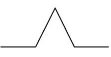
What algorithm fills the shape using the point?
=

~
~
~
~No right answer.
-
What are the parts required to build a standard RS-trigger chip (asynchronous RS-trigger) using the bipolar transistors and NOR schemes?
~One transistor
~Two transistors
~Three transistors
=Four transistors
~No right answer
-
What did the least complicated among the revised adder chips for the two same-order addition contain?
=Three transistors
~Ten transistors
~31 Transistors
~25 transistors
~No right answer
-
What does the difference's order of the output always match for the single-order adder-subtractor chip performing both adding and subtraction?
~Multiplication result of the same orders
~Division result of the same orders
~Square root's calculation result
=Addition result of two same orders
~No right answer
-
What does the PC's TLB buffer contain?
~Random numbers not connected to the program execution
~Identificators' table generated during the compilation time
=Recently accessed virtual tables' ids
~Virtual addresses of the executing program's elements
~Commands of the executing program
-
What does the simplest RS-trigger scheme contain?
=Two complementary outputs, one of which is main
~Three complementary outputs with three of which are main
~Four complementary outputs with four of which are main
~RS-trigger doesn't contain any outputs
~No right answer
-
What does the TLB buffer allow?
~Increase the CPU speed
~Increase the disc operation speed
~Decrease the CPU's tasks execution speed
=Faster conversion from virtual to physical addresses
~No right answer
-
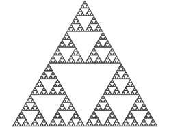
What is a fractal?
=A fractal is a mathematical set that has a fractal dimension that usually exceeds its topological dimension and may fall between the integers. And a parent element is similar to a child.
~A fractal is the process of repeating items in a self-similar way.
~A fractal is a mathematical set that is repeated recursively.
~A fractal is a recursive process of creating shapes.
~No right answer.
-
What is the cause for the necessity for introduction of the cache chip into the CPU <-> Main memory interaction system?
~Slow CPU operation
~Fast CPU and fast memory operation
~Slow CPU and fast memory operation
=Big memory access time compared to the CPU's operation time.
~No right answer
-
What is the child element (motif) of the Koch Curve?
=
~
~
~
~No right answer.
-
What is the child element (motif) of the Koch Island?
~
=

~
~
~No right answer.
-
What is the child element (motif) of the Koch Snowflake?
=

~
~
~
~No right answer.
-
What is the formula for defining a Z-multiplexor (see pic.)
 with two operation outputs α,βand appropriate x1, x2, x3, x4 data
inputs?
with two operation outputs α,βand appropriate x1, x2, x3, x4 data
inputs?
~![]()
=
![]()
~![]()
~![]()
~No right answer
-
What is the input combination J = 1, K = 1 for the JK-trigger chip?
=It is always allowable
~It is allowable in some cases
~There is no chip called JK-trigger
~It is illegal
~No right answer
-
What is the input ports' combination R = 1, S = 1 for the RS-trigger chip?
~The combination is always allowable
~The combination is allowable in some cases
~There is no chip called RS-trigger
=The combination is always illegal
~No right answer
-
What is the Koch Curve?
=

~
~
~
~No right answer.
-
What is the Koch Island?
~
=

~
~
~No right answer.
-
What is the Koch Snowflake?
~
~
=

~
~No right answer.
-
What is the output of the single-order ALU for the fixed set of α, β
=Result of the one operation
~Result of the two operations
~Result of the three operations
~Result of the four operations
~No right answers
-
What is the result of the input combination J = 1, K = 1 for the JK-trigger chip?
~Always zero output.#
~Always one (1) output#
~There is no chip called JK-trigger#
=Inverted value of the previous trigger's output#
~No right answer#
-
What output set does the decoder activate according to the value of its n inputs?
~zero set
~unit set
~half-zero, half-unit set
=one-unit, all remaining zeros set
~No right answer
-
When performing algebraic operations "addition" and "subtraction" of the floating-point numbers is required to determine what the internal operation is required to perform effectively over the mantissa m1 and m2. If the numbers have different signs, and the external operation is subtraction, the internal operation of the mantissa
~multiplication
~division
=addition
~subtraction
~no right answer
-
When performing algebraic operations "addition" and "subtraction" of the floating-point numbers is required to determine what the internal operation is required to perform effectively over the mantissa m1 and m2. If the numbers have same signs, and external operations on numbers is subtraction, than the internal operation on the mantissa{
~multiplication
~division
=subtraction
~addition
~no right answer
-
When performing algebraic operations "addition" and "subtraction" of the floating-point numbers is required to determine what the internal operation is required to perform effectively over the mantissa m1 and m2. If the numbers have different signs, and external operations on numbers is addition, than the internal operation on the mantissa{
~multiplication
~division
=subtraction
~addition
~no right answer
-
When performing algebraic operations "addition" and "subtraction" of the floating-point numbers is required to determine what the internal operation is required, in fact performed on the mantissa M1 and M2. If the numbers have the same sign, and the addition of a foreign operation, the internal operation{
~subtraction
~multiplication
=addition
~division
~no right answer
-
When performing arithmetic operations on two machines (normalized) numbers with the internal operation of subtraction, if the alignment order is not happening, then you can immediately implement the subtraction in column major negative consequence of such a deduction is
~Always doesn't return any result
~Always need to check the extra lower bit mantissa adder
=Loss of the normalization of the result and the need to normalize the "left" with a simultaneous decrease in the number of adder-order equal to the number of digits, which is a shift
~No right answer
~Normalization is always one bit to the right
-
When you perform an operation (addition, subtraction) of two machine numbers in the lower order leveling orders increased to a greater number of the mantissa, and a smaller order{
~Shifts to the left in the register
~Adds with second number's mantissa
=Shifts to the right in the register by the number of bits equal to difference of orders
~Reset
~No right answer
-
When you perform an operation (addition, subtraction) of two machine numbers, after cleaning and loading the operand registers for operands and registers its internal operations, the control unit determines the difference p1-p2 - order operands. If p1-p2\= 0 then "stacked" the corresponding operation is performed on the mantissa, otherwise, if p1 !\= p2, then before the addition of the mantissas is required to make{
~rounding the result of the operation
~add in a column mantissa operand (!m1, !m2)
=alignment operation orders, increasing the smaller of them till bigger
~clean registers
~no right answer
-
Where is the PC's virtual memory situated?
~on the -1 level (sub-physical layer)
~on the zero level (physical layer)
~on the second layer (micro-command layer)
=in the operating system layer
~No right answer
-
Which scheme is required for performing the operation selection for the single-order ALU and 8-bit operation?
~Multiplexor scheme
=3-input decoder
~2-input decoder
~Comparator
~No right answer
-
With the addition of two machine numbers overflow the mantissa adder, which will require in this case, the normalization of the mantissa adder to the right level of 1 bit, the main discharge number mantissa adder will be in the junior secondary discharge. If it is "1" then the operation may be necessary to
~subtraction of "1" from the lower primary level mantissa adder
~subtracting "1" of the higher main discharge mantissa
=rounding, adding 1 to the lowest category of the main mantissa adder
~No right answer
~subtracting "1" from the order of the adder
-
With the addition of two machine numbers, the sum of the mantissas may be greater than 1 (overflow the mantissa adder) to save this "1" is the highest extra bit mantissa adder. This situation requires
~only shift the mantissa adder for a bit "left"
~only shift the mantissa adder, including a senior level in an extra digit to the right(normalized to the right)
=shift the mantissa adder, including her eldest extra bit for a bit to the right and a simultaneous increase in the order of 1 results
~reset the mantissa of the operands
~No right answer
-
Define the action in correct way that takes place in execute cycle.
=Processor-memory\: -> Data may be transferred from processor to memory or from memory to processor.
=Processor-I/O\: -> Data may be transferred to or from a peripheral device by transferring between the processor and an I/O module.
=Data processing\: -> The processor may perform some arithmetic or logic operation on data.
=Control\: -> An instruction may specify that the sequence of execution be altered.
-
Define the steps of Fetch cycle in correct way
=Step 1 -> Program Counter (PC) holds address of next instruction to fetch
=Step 2 -> Processor fetches instruction from memory location pointed to by PC
=Step 3 -> Increment PC
=Step 4 -> Instruction loaded into Instruction Register (IR)
=Step 5 -> Processor interprets instruction and performs required actions
-
Indicate the functionalities according to types of transfers.
=Memory to CPU\: -> The CPU reads an instruction or unit of data from memory.
=CPU to Memory\: -> The CPU writes a unit of data to memory.
=I/O to CPU\: -> The CPU reads data from I/O device via an I/O module.
=CPU to I/O\: -> The CPU sends data to the I/O device.
=I/O to or from the Memory\: -> For these two cases, an I/O module is allowed to exchange data directly with memory, without going through the CPU, using direct memory access (DMA).
-
Match the levels to appropriate functionality
=Level 5 -> High-level language
=Level 4 -> Assembly language level
=Level 3 -> Operating system level
=Level 2 -> Architecture command level
=Level 1 -> Micro-architecture level
=Level 0 -> Digital-logical level
-
A block of data associated with a cache tag and the unit of transfer between cache and memory.
~Cache bridge
=Cache line
~Cache memory
~Cache tag
~Cache memory
-
A bus that connects major computer components is called ____________.
=a system bus
~high performance bus
~a PCI bus
~an expansion bus
~a local bus
-
A communication pathway connecting two or more devices is known as a _____________.
~instruction
~interrupt
=bus
~memory
~register
-
A complete microcomputer system consist of:
I. Microprocessor
II. Memory
III. Peripherals
~I only
~I and II
=I, II and III
~II and III
~I and III
-
A computer program that converts an entire program into machine language is known as a( n ) ______________.
~interpreter
~simulator
=compiler
~commander
~translator
-
A computer-oriented language whose instructions are usually in one-to-one cor- respondence with computer instructions and that may provide facilities such as the use of macroin- structions.
=Assembly language
~High-level language
~Instruction language
~Functional language
~Object-oriented language
-
A condition, usually created by the CPU, during which the CPU will ignore interrupt request signals of a specified class.
=disabled interrupt
~deleted interrupt
~enabled interrupt
~created interrupt
~suspended interrupt
-
A condition, usually created by the CPU, during which the CPU will respond to interrupt request signals of a specified class.
~disabled interrupt
~deleted interrupt
=enabled interrupt
~created interrupt
~suspended interrupt
-
A device attached to a bus that is capable of initiating and controlling communication on the bus.
~bus tree
~bus slave
~bus child
=bus master
~super bus
-
A disk that uses optical technology but that can be easily erased and rewritten. A typical capacity is 650 Mbytes.
~CD
~CD-ROM
~DVD
~WORM
=Erasable Optical Disk
-
A flat circular plate with a magnetizable surface layer, on one or both sides of which data can be stored is known as _________.
=Magnetic disk
~Magnetic tape
~Internal disk
~Hard disk
~Cache memory
-
A functional device which permits to two or more channels of data link to use the same common device of data transfer jointly is known as _____________.
=Multiplexer
~Dedicator
~Timer
~Encoder
~Decoder
-
A functional part of Computer System which is intended for accepting, storing and presentation of data is knowns as a ( n ) ______________.
~Interrupt
=Memory
~Instruction
~Screen
~Bus
-
A memory whose storage locations are identified by their contents, or by a part of their contents, rather than by their names or positions is known as a( n ) ________________.
~Control memory
~Read only memory
~Instruction memory
=Associative memory
~None of the statements
-
A microprogram written as a combination of 0's and 1's is known as a _______________.
~symbolic microinstruction
=binary microinstruction
~decimal microinstruction
~hexadecimal microinstruction
~octal microinstruction
-
A nonerasable disk that stores digitized audio information. The standard system uses 12-cm disks and can record more than 60 minutes of uninterrupted playing time.
=CD
~CD-ROM
~DVD
~WORM
~Erasable Optical Disk
-
A nonerasable disk used for storing computer data. The standard system uses 12-cm disks and can hold more than 550 Mbytes.
~CD
=CD-ROM
~DVD
~WORM
~Erasable Optical Disk
-
A portion of a system bus used for the transfer of an address. Typically, identifies a main memory location or an I/O device.
~control bus
=address bus
~data bus
~PCI bus
~SCSI bus
-
A program whose function is to start the computer software operating when power is turned on is known as a( n ) ____________.
=Bootstrap loader
~Operating System
~Firewall
~Loader
~All of the statements
-
A RAM whose cells are implemented using capacitors. This RAM will gradually lose its data unless it is periodically refreshed.
=Dynamic
~Static
~Firm
~Random
~Associative
-
A RAM whose cells are implemented using flip-flops. This RAM will hold its data as long as power is supplied to it; no periodic refresh is required.
~Dynamic
=Static
~Firm
~Random
~Associative
-
A ratio of all hits in the cache to the number of CPU’s accesses to the memory is called ______________.
=Hit ratio
~Miss ratio
~Success ratio
~Access ratio
~Fraction ratio
-
A register that is used to hold an instruction for interpretation.
=Instruction Register
~Memory Address Register
~Memory Buffer Register
~Program Counter
~Accumulator
-
A relatively small fast memory interposed between a larger, slower memory and the logic that accesses the larger memory. It recently accessed data, and is designed to speed up subsequent access to the same data.
=Cache
~Bus
~Register
~RAM
~ROM
-
a set of electric pathways and service electronic devices (framing), providing exchange of data among computer units and devices is known as a ( n ) ____________.
~instruction
~interrupt
=bus
~memory
~register
-
A set of logically consecutive strips that maps exactly one strip to each array member is referred to as ___________.
~arrays
~sectors
=stripes
~track number
~gaps
-
A single hardware device known as the bus controller (or arbiter) is responsible for allocating time on the bus.
~Dedicated
~Multiplexed
~Timing
~Physically Dedicated
=Centralised
-
A source program is usually written in which language?
~Assembly language
~Machine level language
=High-level language
~Natural language
~Digital-level language
-
A tape with a magnetizable surface layer on which data can be stored by magnetic recording is known as _________.
~Magnetic disk
=Magnetic tape
~Internal disk
~Hard disk
~Cache memory
-
A technique in which the occurrence of events on a bus is determined by a clock. The clock defines equal-width time slots, and events begin only at the beginning of a time slot.
=synchronous timing
~asynchronous timing
~dedicated bus
~multiplexed bus
~physically dedicated
-
A technique in which the occurrence of one event on a bus follows and depends on the occurrence of a previous event.
~synchronous timing
=asynchronous timing
~dedicated bus
~multiplexed bus
~physically dedicated
-
An electronic circuit that produces an output signal that is a simple Boolean operation on its input signals.
=Gate
~Transistor
~Resistor
~Illuminator
~All of the statements
-
An exception conditions in a computer system caused by an event external to the CPU is known as a( n ) ___________.
=interrupt
~write policy
~I/O module
~external memory
~process
-
During the execution of a program which register gets initialized first?
~MBR
~MAR
=PC
~IR
~IAR
-
For what does the ENIAC stand for?
=Electronic Numerical Integrator And Computer
~Electric Numerical Integrator And Computer
~Electronic Numerical International And Computer
~Electric Numerical International And Computer
~Electronic Numerical Integrator Accumulator Computer
-
High-speed memory internal to the CPU.
~ALU
=Register
~Transistor
~Control Unit
~Instruction Register
-
How does the Nested Multiple Interrupts work?
~Interrupts are handled in strict sequential order
=Defines priorities for interrupts and allows an interrupt of higher priority to cause a lower- priority interrupt handler to be itself interrupted.
~Interrupts are handled in odd or even order
~Defines priorities for interrupts and allows an interrupt of lower- priority to cause a higher priority interrupt handler to be itself interrupted.
~None of the statements
-
How does the Sequential Multiple Interrupts work?
=Interrupts are handled in strict sequential order
~Defines priorities for interrupts and allows an interrupt of higher priority to cause a lower- priority interrupt handler to be itself interrupted.
~Interrupts are handled in odd or even order
~Defines priorities for interrupts and allows an interrupt of lower- priority to cause a higher priority interrupt handler to be itself interrupted.
~None of the statements
-
How does the write-through procedure work?
~To write onto the memory directly
~To write and read from memory simultaneously
=To write directly on the memory and the cache simultaneously
~To write and read from cache simultaneously
~To write onto the cachedirectly
-
How many bits in a single byte?
~2
~4
=8
~16
~32
-
In CD-ROM which field contains the block address and the mode byte?
~Sync
=Header
~Data
~Auxiliary
~Track number
-
In CD-ROM which field identifies the beginning of a block?
=Sync
~Header
~Data
~Auxiliary
~Track number
-
In Centralised Arbitration which device(s) is/are is the bus master?
I. Processor
II. DMA controller
III. RAM
~I only
=I and II
~II only
~I and III
~I, II and III
-
In magnetic disk data are transferred to and from the disk in ____________.
~streams
=blocks
~piece
~gaps
~tracks
-
In magnetic disks data are stored in block-size regions known as _____________.
~tracks
=sectors
~gaps
~heads
~bytes
-
In synchronous bus, the devices get the timing signals from
~Timing generator in the device
=A common clock line
~Timing signals are not used at all
~None of the above
~The previous signal
-
In which access method access is accomplished by direct access to reach a general vicinity plus sequential searching, counting, or waiting to reach the final location?
~Sequential
=Direct
~Random
~Associative
~None of the statements
-
In which access method any location can be selected at random and directly addressed and accessed?
~Sequential
~Direct
=Random
~Associative
~None of the statements
-
In which cache state he line in the cache does not contain valid data?
~Modified
~Exclusive
~Shared
=Invalid
~Asynchronous
-
In which cache state the line in the cache has been modified and it differs from that in the main memory, so it is available only in this cache?
=Modified
~Exclusive
~Shared
~Invalid
~Asynchronous
-
In which cache state the line in the cache is the same as that in the main memory and also is not present in any other cache?
~Modified
=Exclusive
~Shared
~Invalid
~Asynchronous
-
In which cache state the line in the cache is the same as that in the main memory and may be present in another cache?
~Modified
~Exclusive
=Shared
~Invalid
~Asynchronous
-
In Winchester Disk Track which component holds the control sum of the field?
~ID field
~SYNCH byte
~Gap
~Data field
=CRC
-
In Winchester Disk Track which component identifies a head, since this disk has multiple surfaces?
~ID field
~SYNCH byte
~Gap
~Data field
=Track number
-
In Winchester Disk Track which component is special bit pattern that determines the beginning of the field?
~ID field
=SYNCH byte
~Gap
~Data field
~CRC
-
In Winchester Disk Track which component is unique identifier or address used to locate a particular sector?
=ID field
~SYNCH byte
~Gap
~Data field
~CRC
-
In ________ protocol the information is directly written into main memory.
=Write through
~Write back
~Write first
~Write again
~Write direct
-
Indicate functions of the computer system
~Data processing
~Data storage
~Data movement
~Control
=All of the statements
-
Mechanism by which other modules (e.g. I/O, memory) may interrupt normal sequence of processing is known as _______________.
=interrupt
~instruction
~fetch
~execute
~operation
-
Memory in which each addressable location has a unique addressing mechanism. The time to access a given location is independent of the sequence of prior access.
~ROM
~PROM
=RAM
~EEPROM
~All of the statements
-
Memory unit that communicates directly with the CPU is called the ______________.
~Auxiliary memory
=Main memory
~Secondary memory
~Register
~Bus memory
-
Metal or plastic disk coated with magnetizable material is known as a( n ) _________________.
=Magnetic Disk
~ROM
~Optical Disk
~Magnetic Tape
~Cache Memory
-
No central controller. Instead each module has access control logic and the modules act together to share the bus.
~Dedicated
~Multiplexed
=Distributed
~Physically Dedicated
~Centralised
-
Numbers and encoded characters generally used as operands is known as a( n ) ____________.
~Input
=Data
~Bits
~Information
~Value
-
One type of an optical disk that is more easily written than CD-ROM, making single-copy disks commercially feasible; holds from 200 to 800 Mbytes of data.
~CD
~CD-ROM
~DVD
=WORM
~Erasable Optical Disk
-
Optical multi-level storage implemented for video with very high capacity?
~CD
~CD-ROM
=DVD
~WORM
~Erasable Optical Disk
-
Optical storage originally implemented for audio where data is stored as pits and data is read by reflecting laser?
~CD
=CD-ROM
~DVD
~WORM
~Erasable Optical Disk
-
Program Counter (PC) is also called ______________.
=Instruction pointer
~Memory pointer
~Data counter
~File pointer
~Instruction counter
-
PROM stands for
=Programmable Read Only Memory.
~Pre-fed Read Only Memory.
~Pre-required Read Only Memory.
~Programmed Read Only Memory.
~Post Read Only Memory
-
Rate at which data can be transferred into or out of a memory unit. is known as a ( n ) _____________.
~Memory cycle time
~Access time
=Transfer rate
~Propagation delay
~Performance time
-
Semiconductor memory whose contents cannot be altered, except by destroying the storage unit. Nonerasable memory.
=ROM
~PROM
~RAM
~EEPROM
~All of the statements
-
Software that controls the execution of programs and that provides services such as resource allocation, scheduling, input/output control, and data management.
=Operating system
~Task Manager
~BIOS
~Operation code
~None of the statement
-
State whether the following statement is True or False for cache memory.
nI. Cache memories are high-speed buffers which are inserted between the processors and main memory.
nII. They can also be inserted between main memory and mass storage.
nIII. It can be used as secondary memory.{
~True, False, True
~False, True, True
=True, True, False
~False, False, True
~True, True, True
-
Storage used to compensate for a difference in rate of flow of data, or time of occurrence of events, when transferring data from one device to another is known as _______________.
=Buffer
~Register
~Program Counter
~Accumulator
~Transistor
-
That portion of the instruction cycle during which the CPU checks for interrupts. If an enabled interrupt is pending, the CPU saves the current program state and resumes processing at an interrupt-handler routine.
~Instruction cycle
~Execute cycle
~Fetch cycle
=Interrupt cycle
~None of the statement
-
That portion of the instruction cycle during which the CPU fetches from memory the instruction to be executed.
~Instruction cycle
~Execute cycle
=Fetch cycle
~Interrupt cycle
~None of the statement
-
That portion of the instruction cycle during which the CPU performs the operation specified by the instruction opcode.
~Instruction cycle
=Execute cycle
~Fetch cycle
~Interrupt cycle
~None of the statement
-
The access time is sum of which of the following? (два ответа сразу выбрать)
~%50%Seek time
~%50%Rotational latency
~Propagation delay
~Unit of transfer
~Serial recording time
-
The algorithm that replaces block in the set that has been in the cache longest is known as ___________.
=First in first out (FIFO)
~Least frequently used (LFU)
~Least Recently used (LRU)
~Random
~None of the statements
-
The algorithm that replaces block in the set that has been in the cache longest with no reference to it is known as ___________.
~First in first out (FIFO)
~Least frequently used (LFU)
=Least Recently used (LRU)
~Random
~None of the statements
-
The algorithm that replaces block in the set that has experienced the fewest references is known as ___________.
~First in first out (FIFO)
=Least frequently used (LFU)
~Least Recently used (LRU)
~Random
~None of the statements
-
The algorithm to remove and place new contents into the cache is called _______.
~Updating algorithm
~Renewal algorithm
=Replacement algorithm
~Refreshing algorithm
-
The classification of buses into synchronous and asynchronous is based on
~The devices connected to them
~The type of data transfer
=The Timing of data transfers
~The bus-hierarchy level
~The type of bus
-
The contents of the EPROM are earsed by
~Overcharging the chip.
=Exposing the chip to UV rays.
~Exposing the chip to IR rays.
~Discharging the Chip.
~Exposing the chip to X-ray rays.
-
The control unit controls other units by generating __________.
~Control signals
=Timing signals
~Transfer signals
~Command Signals
~I/O Signals
-
The correspondence between the main memory blocks and those in the cache is given by _________.
~Hash function
=Mapping function
~Locale function
~Assign function
~Digest function
-
The delays caused in the switching of the timing signals is due to
~Memory access time
~WMFC
=Propagation delay
~Processor delay
~All of the statements
-
The device which starts data transfer is called __________.
~Master
~Transactor
~Slave
=Initiator
~Distributer
-
The disk system consists of which of the following:
I Disk
II Disk drive
III Disk controller
~I only
~I and II
=I,II and III
~II and III
~I and III
-
The drawback of building a large memory with DRAM is
~The large cost factor.
~The inefficient memory organisation.
=The slow speed of operation.
~They require specially designed CPU.
~All of the statements
-
The effectiveness of the cache memory is based on the property of ________.
=Locality of reference
~Memory localisation
~Memory size
~Memory type
~Memory capacity
-
The first major change in the electronic computer came with the replacement of the vacuum tube by the _____________
=transistor
~resistor
~registor
~accumulator
~None of the statements
-
The key factor(s) in commercial success of a computer is(are) ________.
~%50%Performance
~Speed
~Design
~%50%Cost
~Color
-
The main virtue for using single Bus structure is ___________ .
~Fast data transfer
~Cost effective connectivity and speed
=Cost effective connectivity and ease of attaching peripheral devices
~No propagation delays
~Reliable data transfer
-
The memory blocks are mapped on to the cache with the help of ______.
~Hash functions
~Replacment algorithm
=Mapping functions
~Write policy
~Data consistency
-
The memory devices which are similar to EEPROM but differ in the cost effectiveness is ______.
~Memory sticks
~Blue-ray devices
=Flash memory
~CMOS
~HDD
-
The method of mapping the consecutive memory blocks to consecutive cache blocks is called ______.
~Set associative
~Associative
=Direct
~Indirect
~MESI
-
The NOR gate is complement of which gate?
~AND
=OR
~XOR
~NAND
~NOT
-
The number failed attempts to access memory, stated in the form of fraction is called as _____________.
~Hit rate
=Miss rate
~Failure rate
~Access rate
~Successful fraction
-
The number successful accesses to memory stated as a fraction is called as __________.
=Hit rate
~Miss rate
~Success rate
~Access rate
~Successful fraction
-
The operation of each individual component as part of the structure is known as _______________.
~Structure
=Function
~Control mechanism
~Apparatus
~Data storage
-
The process of determining which competing bus master will be permitted access to the bus.
~bus controlling
=bus arbitration
~data bus lines
~bus prediction
~bus identification
-
The processing required for a single instruction is called a( n ) _______________
=instruction cycle
~fetch cycle
~execute cycle
~program counter
~Input/Output
-
The PROM is more effective than ROM chips in regard to which of the following
I. Cost
II. Memory management
III. Speed of operatioт
~I only
~I and II
~II only
=I and III
~I, II and III
-
The reason for the implementation of the cache memory is
~To increase the internal memory of the system
=The difference in speeds of operation of the processor and memory
~ To reduce the memory access and cycle time
~To increase the storage capacity of computer
~All of the statements
-
The registers, ALU and the interconnection between them are collectively called as _______________.
~Process path
~Information path
=Data path
~Control path
~CU path
-
The ROM chips are mainly used to store _______.
~Root files
~System files
=Boot files
~Driver files
~Operating system files
-
The small extremely fast, RAM’s are called as ___________.
~Heaps
~Accumulators
~Registers
=Cache
~Internal memory
-
The technology of video-signals recording and other data of a large volume is used and it’s based on methods of information (data) compression.
~CD
~CD-ROM
=DVD
~WORM
~Erasable Optical Disk
-
The time delay between two successive initiation of memory operation _____________.
~Memory access time
~Memory search time
=Memory cycle time
~Instruction delay
~Propagation delay
-
The time that elapses between the initiation of an operation and completion of that operation is called _____________.
~throughput
~memory response time
=memory access time
~execution time
~unit of transfer
-
The time that is taken for the sector to reach the head is known as _______________.
~reach the head time
=rotational latency
~seek time
~disk access time
~unit of transfer
-
The time that is taken to position the head at the track is known as _____________.
~access time
~unit of transfer
=seek time
~track time
~positioning time
-
The unit which decodes and translates each instruction and generates the necessary enable signals for ALU and other units is known as a ( n ) ______________.
~arithmetic unit
~logical unit
=control unit
~internal bus
~CPU
-
The way in which the components are interrelated is known as _______________.
=Structure
~Function
~Operation
~Apparatus
~Data storage
-
The __________________ is a group of bits that instruct the computer to perform a specific operation. It is usually divided into parts, each having its own particular interpretation.
=instruction code
~program counter
~accumulator
~magnitude
~address
-
The “natural” unit of organization of memory is known as a ( n ) _________.
~Byte
=Word
~Sequence
~Address
~Bits
-
Time between presenting the address and getting the valid data (for random access) is known as a ( n ) _____________.
~Memory cycle time
=Access time
~Transfer rate
~Propagation delay
~Performance time
-
Time may be required for the memory to “recover” before next access is known as a ( n ) _____________.
=Memory cycle time
~Access time
~Transfer rate
~Propagation delay
~Performance time
-
To distinguish between two sectors in disks we make use of _____________.
=Inter sector gap
~Splitting bit
~Numbering bit
~Track number
~Surface spots
-
To extend the connectivity of the processor bus we use ______ .
=PCI bus
~SCSI bus
~ Controllers
~Multiple bus
~System bus
-
To reduce the memory access time which of the following internal memory is used?
~SRAM
~DRAM
=Cache
~ROM
~PROM
-
To resolve the clash over the access of the system BUS we use __________ .
~Multiple Bus
=Bus arbitrator
~Priority access
~Sequential access
~PCI bus
-
To which of the following possible type of operations do the following view depict?
=Data movement
~Data storage
~Either data processing and data storage
~Processing from storage to I/O
~Processing from/to storage
-
To which of the following possible type of operations do the following view depict?
~Data movement
=Data storage
~Either data processing and data storage
~Processing from storage to I/O
~Processing from/to storage
-
To which of the following possible type of operations do the following view depict?
~Data movement
~Data storage
~Neither data processing nor data storage
~Processing from storage to I/O
=Processing from/to storage
-
To which of the following possible type of operations do the following view depict?
~Data movement
~Data storage
~Neither data processing nor data storage
=Processing from storage to I/O
~Processing from/to storage
-
What does the Capacity characteristic of memory define?
~Refers to whether memory is internal and external to the computer.
=Defines number of words for internal memory and number of bytes for external memory.
~Defines the number of electrical lines into and out of the memory module.
~Refers to the method of accessing data according to the structure of the memory.
~Defines the performance of the memory.
-
What does the Location characteristic of memory define?
=Refers to whether memory is internal and external to the computer.
~Defines number of words for internal memory and number of bytes for external memory.
~Defines the number of electrical lines into and out of the memory module.
~Refers to the method of accessing data according to the structure of the memory.
~Defines the performance of the memory.
-
What does the RAID stands for?
~Redundant Assembly of Independent Disks
=Redundant Array of Independent Disks
~Rotational Array of Independent Disks
~Rotational Assembly of Independent Disks
~None of the statements
-
What does the Unit of transfer characteristic of memory define?
~Refers to whether memory is internal and external to the computer.
~Defines number of words for internal memory and number of bytes for external memory.
=Defines the number of electrical lines into and out of the memory module.
~Refers to the method of accessing data according to the structure of the memory.
~Defines the performance of the memory.
-
What is the role of the Direct Memory Access (DMA)?
=The DMA controls the exchange of data between main memory and an I/O module.
~With the DMA data is exchanged between the CPU and I/O module.
~With the DMA, the CPU issues an I/O command, continues to execute other instructions, and is interrupted by I/O module when the latter has completed work.
~The transfer of a page from auxiliary storage to real storage at the moment of need.
~All of the statements
-
What is the role of the I/O address register (I/OAR) in the CPU?
~specifies the address in memory for the next read or write
~contains the data to be written into memory or receives the data read from memory
=specifies a particular I/O device.
~is used for the exchange of data between an I/O module and the CPU
~All of the statements
-
What is the role of the I/O buffer register (I/OBR) in the CPU?
~specifies the address in memory for the next read or write
~contains the data to be written into memory or receives the data read from memory
~specifies a particular I/O device.
=is used for the exchange of data between an I/O module and the CPU
~All of the statements
-
What is the role of the Interrupt-driven I/O?
~The Interrupt-driven I/O controls the exchange of data between main memory and an I/O module.
~With the Interrupt-driven I/O data is exchanged between the CPU and I/O module.
=With the Interrupt-driven I/O, the CPU issues an I/O command, continues to execute other instructions, and is interrupted by I/O module when the latter has completed work.
~The transfer of a page from auxiliary storage to real storage at the moment of need.
~All of the statements
-
What is the role of the memory address register (MAR) in the CPU?
=specifies the address in memory for the next read or write
~contains the data to be written into memory or receives the data read from memory
~specifies a particular I/O device.
~is used for the exchange of data between an I/O module and the CPU
~All of the statements
-
What is the role of the memory buffer register (MBR) in the CPU?
~specifies the address in memory for the next read or write
=contains the data to be written into memory or receives the data read from memory
~specifies a particular I/O device.
~is used for the exchange of data between an I/O module and the CPU
~All of the statements
-
What is the role of the Programmed I/O?
~The Programmed I/O controls the exchange of data between main memory and an I/O module.
=With the Programmed I/O data is exchanged between the CPU and I/O module.
=With the Programmed I/O, the CPU issues an I/O command, continues to execute other instructions, and is interrupted by I/O module when the latter has completed work.
~The transfer of a page from auxiliary storage to real storage at the moment of need.
~All of the statements
-
What's the role of Arithmetic and logic unit (ALU) in computer?
~Stores data
~Moves data between the computer and its external environment
~Provides for communication among CPU, main memory, and I/O
~Controls the operation of the CPU and hence the computer
=Performs the computer’s data processing functions
-
What's the role of Control unit in computer?
~Stores data
~Moves data between the computer and its external environment
~Provides for communication among CPU, main memory, and I/O
=Controls the operation of the CPU and hence the computer
~Performs the computer’s data processing functions
-
What's the role of CPU interconnection in computer?
=Provides for communication among the control unit, ALU, and registers
~Moves data between the computer and its external environment
~Provides for communication among CPU, main memory, and I/O
~Controls the operation of the CPU and hence the computer
~Performs the computer’s data processing functions
-
What's the role of I/O in computer?
~Stores data
=Moves data between the computer and its external environment
~Provides for communication among CPU, main memory, and I/O
~Controls the operation of the CPU and hence the computer
~Performs the computer’s data processing functions
-
What's the role of Main memory in computer?
=Stores data
~Moves data between the computer and its external environment
~Provides for communication among CPU, main memory, and I/O
~Controls the operation of the CPU and hence the computer
~Performs the computer’s data processing functions
-
What's the role of Registers in computer?
=Provides storage internal to the CPU
~Moves data between the computer and its external environment
~Provides for communication among CPU, main memory, and I/O
~Controls the operation of the CPU and hence the computer
~Performs the computer’s data processing functions
-
What's the role of System interconnection in computer?
~Stores data
~Moves data between the computer and its external environment
=Provides for communication among CPU, main memory, and I/O
~Controls the operation of the CPU and hence the computer
~Performs the computer’s data processing functions
-
Which access method enables to make a comparison of desired bit locations within a word for a specified match, and to do this for all words simultaneously?
~Sequential
~Direct
~Random
=Associative
~None of the statements
-
Which access method starts at the current position and reads through in order?
~Direct
~Associative
~Random
=Sequential
~None of the statement
-
Which bus buffers data circulating between the Main Memory and peripheral devices’ controllers allows to support a large variety of external devices?
~Local Bus
~System Bus
=Expansion Bus
~High-Speed Bus
~PCI Bus
-
Which bus type assigned to a single function (e.g. address bus) or a physical subset of components (e.g. I/O bus connects all I/O modules).
=Dedicated
~Multiplexed
~Timing
~Physically Dedicated
~Centralised
-
Which bus type can be used for both addresses and data. In this case, an address valid control line is needed to determine whether the data is an address or data.
~Dedicated
=Multiplexed
~Timing
~Physically Dedicated
~Centralised
-
Which bus unites high-speed external devices and is connected with the System Bus through special concordance module - Bridge.
~Local Bus
~System Bus
~Expansion Bus
=High-Speed Bus
~PCI Bus
-
Which component controls the operation of the computer and performs its data processing functions?
=Central Processing Unit (CPU)
~Main memory
~I/O devices
~System interconnection
~Control unit
-
Which component Moves data between the computer and its external environment?
~Central Processing Unit (CPU)
~Main memory
=I/O devices
~System interconnection
~Control unit
-
Which computer was designed and constructed at the University of Pennsylvania, was the world’s first general- purpose electronic digital computer.
=ENIAC
~EDVAC
~IAS
~THE VON NEUMANN MACHINE
~All of the statements
-
Which memory device is generally made of semi-conductors?
=RAM
~Hard-disk
~Floppy disk
~CD
~DVD
-
Which memory device is NOT generally made of semi-conductors?
~RAM
~Cache
~Register
=CD
~ROM
-
Which of one of the following is NOT TRUE?
~ key charac- teristic of a bus is that it is a shared transmission medium.
~Multiple devices connect to the bus.
~A signal transmitted by any one device is available for reception by all other devices attached to the bus.
~Only one device at a time can successfully transmit.
=Multiple devices at a time can successfully transmit.
-
Which of the following are bus types?
~Centralized
~%50%Dedicated
~Distributed
~%50%Multiplexed
~Synchronous
-
Which of the following are characteristics of magnetic tape?
~%25%Serial access is used for reading data
~%25%Slow
~%25%Very cheap
~%25%Generally used for backup and archive
~Uses multi-layer technology
-
Which of the following are common characteristics shared by different design architectures of RAID?
~RAID is a set of logical disk drives viewed by operating system as a single logical drive.
~%33.333%RAID is a set of physical disk drives viewed by operating system as a single logical drive.
~%33.333%Data is distributed across the physical drives of an array.
~No redundancy
~%33.333%Redundant disk capacity is used to store parity information , which guarantees data recoverability in case of a disk failure.
-
Which of the following are inherent drawbacks of Programmed I/O and Interrupt-driven I/O?
~%50%The I/O transfer rate is limited by the speed with which the CPU can test and service a device.
~%50%The CPU is tied up in managing an I/O transfer; a number of instructions must be executed for each I/O transfer.
~The number of words to be read or written is limited
~To execute I/O-related instruction, the CPU issues an address, specifying the particular module and external device, and I/O command.
~The address of the I/O device is always involved
-
Which of the following are major computer components?
~%33.333%I/O
~HDD drive
~%33.333%Processor
~Power supply
~%33.333%Memory
-
Which of the following are method of arbitration of bus?
~%50%Centralized
~Dedicated
~%50%Distributed
~Multiplexed
~Synchronous
-
Which of the following are single bus problems:
~%50%The more devices attached to the bus, the greater the bus length and hence the greater the propagation delay.
~Each module has its own bus controller which causes signal distribution problem.
~%50%The bus may become a bottleneck as the aggregate data transfer demand approaches the capacity of the bus.
~Single hardware device controlling bus access
~All of the statements
-
Which of the following below is not a component of the computer?
~I/O device
~Main memory
~System bus
~CPU
=External memory
-
Which of the following below is not a component of the CPU?
~Registers
~ALU
~Internal bus
~Control unit
=Main memory
-
Which of the following is (are) component(s) of Control Unit?
I. Sequencing logic
II. Control unit registers and decoders
III. Control memory
IV. Internal registers
=I, II and III
~II, III and IV
~I, II and IV
~I and III
~I, II, III and IV
-
Which of the following is (are) concept(s) of Hardwired Program?
I. Hardwired systems are inflexible
II. General purpose hardware can do different tasks, given correct control signals
III. Instead of re-wiring, supply a new set of control signals
=I, II and III
~I and II
~I and III
~II and III
~None of the statements
-
Which of the following is (are) type(s) of external memory?
~Random Access Memory
~%33.333%Magnetic Disk
~Cache Memory
~%33.333%Optical Disk
~%33.333%Magnetic Tape
-
Which of the following is NOT the operation that CPU performs?
~Logic operation
~Arithmetic operation
=Data transfer
~Data processing
~None of the statements
-
Which of the following is(are) advantage(s) of the transistor over the vacuum tube?
~The transistor is smaller
~The transistor is cheaper
~The transistor dissipates less heat than a vacuum tube
~The transistor is a solid-state device, made from silicon
=All of the statements
-
Which one of the following best describes the functionality of the address lines?
=Are used to designate the source or destination of the data on the data bus.
~Are used to control the access to and the use of the data and address lines.
~Causes data on the bus to be written into the addressed location.
~Causes data on the bus to be output to the addressed I/O port.
~Provide a path for moving data among system modules.
-
Which one of the following best describes the functionality of the control lines?
~Are used to designate the source or destination of the data on the data bus.
=Are used to control the access to and the use of the data and address lines.
~Causes data on the bus to be written into the addressed location.
~Causes data on the bus to be output to the addressed I/O port.
~Provide a path for moving data among system modules.
-
Which one of the following best describes the functionality of the data lines?
~Are used to designate the source or destination of the data on the data bus.
~Are used to control the access to and the use of the data and address lines.
~Causes data on the bus to be written into the addressed location.
~Causes data on the bus to be output to the addressed I/O port.
=Provide a path for moving data among system modules.
-
Which one of the following is the definition of Data Channel?
=Data Channel is an independent I/O block, which is equipped with its own processor and own system of instructions. These instructions are stored in the main memory subsystem, but they are executed only by corresponding processor (of I/O block).
~Data Channel is a device, which serves as a central commutator for data transfer among data channels, CPU and the main memory. It may be considered as a dispatcher (manager) of access to the main memory by CPU and data channels
~Data Channel is an electronic device on the base of semiconductor crystal, which has got three or more electrodes; it intended for amplification, generation or transformation electric oscillations.
~Data Channel is an electronic device made by printing thousands or even millions of tiny transistors and some other electronic elements on a small silicon crystal (chip), which are connected in a certain way and considered as entire one.
~None of the statements
-
Which one of the following is the definition of Integrated circuit?
~Integrated circuit is an independent I/O block, which is equipped with its own processor and own system of instructions. These instructions are stored in the main memory subsystem, but they are executed only by corresponding processor (of I/O block).
~Integrated circuit is a device, which serves as a central commutator for data transfer among data channels, CPU and the main memory. It may be considered as a dispatcher (manager) of access to the main memory by CPU and data channels
~Integrated circuit is an electronic device on the base of semiconductor crystal, which has got three or more electrodes; it intended for amplification, generation or transformation electric oscillations.
=Integrated circuit is an electronic device made by printing thousands or even millions of tiny transistors and some other electronic elements on a small silicon crystal (chip), which are connected in a certain way and considered as entire one.
~None of the statements
-
Which one of the following is the definition of Multiplexor?
~Multiplexor is an independent I/O block, which is equipped with its own processor and own system of instructions. These instructions are stored in the main memory subsystem, but they are executed only by corresponding processor (of I/O block).
=Multiplexor is a device, which serves as a central commutator for data transfer among data channels, CPU and the main memory. It may be considered as a dispatcher (manager) of access to the main memory by CPU and data channels
~Multiplexor is an electronic device on the base of semiconductor crystal, which has got three or more electrodes; it intended for amplification, generation or transformation electric oscillations.
~Multiplexor is an electronic device made by printing thousands or even millions of tiny transistors and some other electronic elements on a small silicon crystal (chip), which are connected in a certain way and considered as entire one.
~None of the statements
-
Which one of the following is the definition of Program Flow Control?
=Program Flow Control is an abstraction at the set of all possible sequences of execution in the program.
~Program Flow Control is a temporary cessation of the process caused by an event, which is an external one as regards to this process.
~Program Flow Control are some changes in the control flow caused not by the program itself, but by something other, and usually connected with the I/O process.
~Program Flow Control is a mechanism by which other modules (e.g. I/O, memory) may interrupt normal sequence of processing.
~All of the statements
-
Which one of the following is the definition of the term Analog Computer?
=A computing device, which processes data given in a form of continuously changing physical values, the meanings of which may be measured
~An electronic computing device, which receives a discrete input data, processes it in accordance with the list of instructions stored inside it and generates resulting output data
~A set of material or abstract objects, which are simultaneously considered as one whole (entire), and which have been united for achieving some certain results.
~A device or a complex of devices, which is intended for mechanization or automating of data processing, and which is constructed on the base of electronic elements
~A detailed instructions that control the operation of a computer system