


7-34 |
The VHDL Cookbook |
use work.dp32_types.all;
entity cond_code_comparator is generic (Tpd : Time := unit_delay); port (cc : in CC_bits;
cm : in cm_bits; result : out bit);
end cond_code_comparator;
architecture behaviour of cond_code_comparator is alias cc_V : bit is cc(2);
alias cc_N : bit is cc(1); alias cc_Z : bit is cc(0); alias cm_i : bit is cm(3); alias cm_V : bit is cm(2); alias cm_N : bit is cm(1); alias cm_Z : bit is cm(0);
b e g i n
result <= bool_to_bit(((cm_V and cc_V)
or (cm_N and cc_N)
or (cm_Z and cc_Z)) = cm_i) after Tpd;
end behaviour;
Figure7-25. Description of the condition code comparator.
7.6.9. Condition Code Comparator
The description of the condition code comparator is listed in Figure7-25. The cc input port contains the three condition code bits V, N and Z, and the cm input contains the four condition mask bits derived from a DP32 instruction. Aliases for each of these bits are declared in the architecture body. The behaviour is implemented by a single concurrent signal assignment statement, which is sensitive to all of the input bits. Whenever any of the bits changes value, the assignment will be resumed and a new result bit computed.
7.6.10.Structural Architecture of the DP32
In this section, a structural architecture body for the DP32 processor, corresponding to Figure7-16, will be described. See Figure7-26 for a listing of the architecture body.

7. Sample Models: The DP32 Processor |
7-35 |
use work.dp32_types.all, work.ALU_32_types.all;
architecture RTL of dp32 is
component reg_file_32_rrw generic (depth : positive);
port (a1 : in bit_vector(depth-1 downto 0); q1 : out bus_bit_32 bus;
en1 : in bit;
a2 : in bit_vector(depth-1 downto 0); q2 : out bus_bit_32 bus;
en2 : in bit;
a3 : in bit_vector(depth-1 downto 0); d3 : in bit_32;
en3 : in bit); end component;
component mux2
generic (width : positive);
port (i0, i1 : in bit_vector(width-1 downto 0); y : out bit_vector(width-1 downto 0); sel : in bit);
end component;
component PC_reg port (d : in bit_32;
q : out bus_bit_32 bus; latch_en : in bit;
out_en : in bit; reset : in bit);
end component;
component ALU_32
port (operand1 : in bit_32; operand2 : in bit_32;
result : out bus_bit_32 bus; cond_code : out CC_bits; command : in ALU_command);
end component;
component cond_code_comparator port (cc : in CC_bits;
cm : in cm_bits; result : out bit);
end component;
component buffer_32 port (a : in bit_32;
b : out bus_bit_32 bus; en : in bit);
end component;
component latch
generic (width : positive);
port (d : in bit_vector(width-1 downto 0);
q : out bit_vector(width-1 downto 0); en : in bit);
end component;
Figure7-26. Structural description of the DP32 processor.

7-36 |
The VHDL Cookbook |
component latch_buffer_32 port (d : in bit_32;
q : out bus_bit_32 bus; latch_en : in bit;
out_en : in bit); end component;
component signext_8_32 port (a : in bit_8;
b : out bus_bit_32 bus; en : in bit);
end component;
signal op1_bus : bus_bit_32; signal op2_bus : bus_bit_32; signal r_bus : bus_bit_32;
signal ALU_CC : CC_bits; signal CC : CC_bits;
signal current_instr : bit_32;
alias instr_a1 : bit_8 is current_instr(15 downto 8); alias instr_a2 : bit_8 is current_instr(7 downto 0); alias instr_a3 : bit_8 is current_instr(23 downto 16); alias instr_op : bit_8 is current_instr(31 downto 24); alias instr_cm : cm_bits is current_instr(19 downto 16);
signal reg_a2 : bit_8; signal reg_result : bit_32;
signal addr_latch_en : bit; signal disp_latch_en : bit; signal disp_out_en : bit; signal d2_en : bit;
signal dr_en : bit;
signal instr_latch_en : bit; signal immed_signext_en : bit; signal ALU_op : ALU_command; signal CC_latch_en : bit;
signal CC_comp_result : bit; signal PC_latch_en : bit; signal PC_out_en : bit; signal reg_port1_en : bit; signal reg_port2_en : bit; signal reg_port3_en : bit;
signal reg_port2_mux_sel : bit; signal reg_res_latch_en : bit;
begin -- architecture RTL of dp32
reg_file : reg_file_32_RRW generic map (depth => 8)
port map (a1 => instr_a1, q1 => op1_bus, en1 => reg_port1_en, a2 => reg_a2, q2 => op2_bus, en2 => reg_port2_en, a3 => instr_a3, d3 => reg_result, en3 => reg_port3_en);
reg_port2_mux : mux2 generic map (width => 8)
port map (i0 => instr_a2, i1 => instr_a3, y => reg_a2, sel => reg_port2_mux_sel);
Figure7-26 (continued).

7. Sample Models: The DP32 Processor |
7-37 |
The architecture refers to the items declared in the packages dp32_types and ALU_32_types, so a use clause for these packages is included. The declaration section of the architecture contains a number of component declarations, corresponding to the entity declarations listed in Sections7.6.1 to7.6.9. Instances of these components are subsequently used to construct the processor architecture.
Next, a number of signals are declared, corresponding to the buses illustrated in Figure7-16. These are followed by further signal declarations for control signals not shown in the figure. The control signals are used to connect the data path component instances with the control unit implemented in the block called controller.
reg_res_latch : latch
generic map (width => 32)
port map (d => r_bus, q => reg_result, en => reg_res_latch_en);
PC : PC_reg
port map (d => r_bus, q => op1_bus,
latch_en => PC_latch_en, out_en => PC_out_en, reset => reset);
ALU : ALU_32
port map (operand1 => op1_bus, operand2 => op2_bus, result => r_bus, cond_code => ALU_CC, command => ALU_op);
CC_reg : latch
generic map (width => 3)
port map (d => ALU_CC, q => CC, en => CC_latch_en);
CC_comp : cond_code_comparator
port map (cc => CC, cm => instr_cm, result => CC_comp_result);
dr_buffer : buffer_32
port map (a => d_bus, b => r_bus, en => dr_en);
d2_buffer : buffer_32
port map (a => op2_bus, b => d_bus, en => d2_en);
disp_latch : latch_buffer_32
port map (d => d_bus, q => op2_bus,
latch_en => disp_latch_en, out_en => disp_out_en);
addr_latch : latch
generic map (width => 32)
port map (d => r_bus, q => a_bus, en => addr_latch_en);
instr_latch : latch
generic map (width => 32)
port map (d => r_bus, q => current_instr, en => instr_latch_en);
immed_signext : signext_8_32
port map (a => instr_a2, b => op2_bus, en => immed_signext_en);
Figure7-26 (continued).
7-38 |
The VHDL Cookbook |
controller : block
port (phi1, phi2 : in bit; reset : in bit; opcode : in bit_8;
read, write, fetch : out bit; ready : in bit; addr_latch_en : out bit; disp_latch_en : out bit; disp_out_en : out bit; d2_en : out bit;
dr_en : out bit; instr_latch_en : out bit; immed_signext_en : out bit;
ALU_op : out ALU_command; CC_latch_en : out bit; CC_comp_result : in bit; PC_latch_en : out bit; PC_out_en : out bit; reg_port1_en : out bit; reg_port2_en : out bit; reg_port3_en : out bit; reg_port2_mux_sel : out bit; reg_res_latch_en : out bit);
port map (phi1 => phi1, phi2 => phi2, reset => reset,
opcode => instr_op,
read => read, write => write, fetch => fetch, ready => ready,
addr_latch_en => addr_latch_en, disp_latch_en => disp_latch_en, disp_out_en => disp_out_en, d2_en => d2_en,
dr_en => dr_en,
instr_latch_en => instr_latch_en, immed_signext_en => immed_signext_en, ALU_op => ALU_op,
CC_latch_en => CC_latch_en, CC_comp_result => CC_comp_result,
PC_latch_en => PC_latch_en, PC_out_en => PC_out_en, reg_port1_en => reg_port1_en,
reg_port2_en => reg_port2_en, reg_port3_en => reg_port3_en, reg_port2_mux_sel => reg_port2_mux_sel, reg_res_latch_en => reg_res_latch_en);
Figure7-26 (continued).

7. Sample Models: The DP32 Processor |
7-39 |
The control unit is a state machine, whose behaviour is described by a single process called state_machine. The controller sequences through the states listed in the declaration of the type controller_state to fetch, decode and execute instructions. The variable state holds the controller state for the current clock cycle, and next_state is set to determine the state for the next clock cycle. Write_back_pending is a flag used to schedule a register write operation for the next clock cycle. The constant ALU_op_select is a lookup table used to determine the ALU function from the instruction op-code.
Figure7-26 (continued).
b e g i n -- block controller
state_machine: process
type controller_state is
(resetting, fetch_0, fetch_1, fetch_2, decode, disp_fetch_0, disp_fetch_1, disp_fetch_2, execute_0, execute_1, execute_2);
variable state, next_state : controller_state; variable write_back_pending : boolean;
type ALU_op_select_table is
array (natural range 0 to 255) of ALU_command;
constant ALU_op_select : ALU_op_select_table := (16#00# => add,
16#01# => subtract, 16#02# => multiply, 16#03# => divide, 16#10# => add, 16#11# => subtract, 16#12# => multiply, 16#13# => divide, 16#04# => log_and, 16#05# => log_or, 16#06# => log_xor, 16#07# => log_mask, others => disable);

7-40 |
The VHDL Cookbook |
The body of the state machine process starts by waiting for the leading edge of the phi1 clock, indicating the start of a clock cycle. When this occurs, the reset signal is checked, and if it is asserted the controller state is set to resetting and all control outputs are negated. On the other hand, if reset is negated, the controller state is updated to the previously computed next state.
b e g i n -- process state_machine
--
--start of clock cycle
wait until phi1 = '1';
--check for reset
--
if reset = '1'then state := resetting;
--
--reset external bus signals
read <= '0'after Tpd; fetch <= '0'after Tpd;
write <= '0'after Tpd;
--reset dp32 internal control signals
addr_latch_en <= '0'after Tpd; disp_latch_en <= '0'after Tpd;
disp_out_en <= '0'after Tpd; d2_en <= '0'after Tpd;
dr_en <= '0'after Tpd; instr_latch_en <= '0'after Tpd;
immed_signext_en <= '0'after Tpd; ALU_op <= disable after Tpd;
CC_latch_en <= '0'after Tpd; PC_latch_en <= '0'after Tpd;
PC_out_en <= '0'after Tpd; reg_port1_en <= '0'after Tpd;
reg_port2_en <= '0'after Tpd; reg_port3_en <= '0'after Tpd;
reg_port2_mux_sel <= '0'after Tpd; reg_res_latch_en <= '0'after Tpd;
--clear write-back flag
--
write_back_pending := false;
--
else -- reset = '0' state := next_state;
end if;
Figure7-26 (continued).

7. Sample Models: The DP32 Processor |
7-41 |
The remainder of the state machine body is a case statement using the current state to determine the action to be performed for this clock cycle. If the processor is being reset (in the resetting state), it waits until the trailing edge of phi2 at the end of the clock cycle, and checks the reset signal again. If reset has been negated, the processor can start fetching instructions, so the next state is set to fetch_0, otherwise it is is set to resetting again.
--
-- dispatch action for current state
--
case state is
when resetting =>
--
-- check for reset going inactive at end of clock cycle
--
wait until phi2 = '0'; if reset = '0'then
next_state := fetch_0; e l s e
next_state := resetting; end if;
--
when fetch_0 =>
--
--clean up after previous execute cycles
reg_port1_en <= '0'after Tpd; reg_port2_mux_sel <= '0'after Tpd;
reg_port2_en <= '0'after Tpd; immed_signext_en <= '0'after Tpd;
disp_out_en <= '0'after Tpd; dr_en <= '0'after Tpd;
read <= '0'after Tpd; d2_en <= '0'after Tpd;
write <= '0'after Tpd;
--handle pending register write-back
--
if write_back_pending then reg_port3_en <= '1'after Tpd;
end if;
--
-- enable PC via ALU to address latch
-- |
|
PC_out_en <= '1'after Tpd; |
-- enable PC onto op1_bus |
ALU_op <= pass1 after Tpd; |
-- pass PC to r_bus |
-- |
|
wait until phi2 = '1'; |
|
addr_latch_en <= '1'after Tpd; |
-- latch instr address |
wait until phi2 = '0'; |
|
addr_latch_en <= '0'after Tpd; |
|
-- |
|
next_state := fetch_1; |
|
-- |
|
Figure7-26 (continued).

7-42 |
The VHDL Cookbook |
The processor fetches an instruction from memory by sequencing through the states fetch_0, fetch_1 and fetch_2 on successive clock cycles. Figure7-27 shows the timing of control signals for an instruction fetch. The fetch_0 processor cycle corresponds to a Ti cycle on the memory bus. During this cycle, the PC register output is enabled onto the op1 bus, and the ALU function set to pass1. The ALU passes the PC value through to the result bus, and it is latched into the memory address register during the
second half of the cycle. The PC value is thus set up on the memory address bus. The fetch_1 cycle corresponds to a memory bus T1 cycle. The controller starts the memory transaction by asserting fetch and read. At the same time, it changes the ALU function code to incr1, causing the ALU to place
when fetch_1 =>
--
--clear pending register write-back
if write_back_pending then reg_port3_en <= '0'after Tpd; write_back_pending := false;
end if;
--increment PC & start bus read
-- |
|
ALU_op <= incr1 after Tpd; |
-- increment PC onto r_bus |
fetch <= '1'after Tpd; |
|
read <= '1'after Tpd; |
|
-- |
|
wait until phi2 = '1'; |
|
PC_latch_en <= '1'after Tpd; |
-- latch incremented PC |
wait until phi2 = '0'; |
|
PC_latch_en <= '0'after Tpd; |
|
-- |
|
next_state := fetch_2; |
|
-- |
|
when fetch_2 => |
|
-- |
|
-- cleanup after previous fetch_1 |
|
-- |
|
PC_out_en <= '0'after Tpd; |
-- disable PC from op1_bus |
ALU_op <= disable after Tpd; |
-- disable ALU from r_bus |
-- |
|
-- latch current instruction |
|
-- |
|
dr_en <= '1'after Tpd; |
-- enable fetched instr onto r_bus |
-- |
|
wait until phi2 = '1'; |
|
instr_latch_en <= '1'after Tpd; |
-- latch fetched instr from r_bus |
wait until phi2 = '0'; |
|
instr_latch_en <= '0'after Tpd; |
|
-- |
|
if ready = '1'then |
|
next_state := decode; |
|
e l s e |
|
next_state := fetch_2; |
-- extend bus read |
end if; |
|
Figure7-26 (continued).

7. Sample Models: The DP32 Processor |
7-43 |
phi1
phi2
PC_out_en
PC_latch_en
addr_latch_en
ALU_op
dr_en
instr_latch_en
a_bus
fetch
read
d_bus
ready
fetch_0 |
fetch_1 |
fetch_2 |
decode |
pass1 |
incr1 |
disable |
|
valid address |
|
|
|
|
|
valid data in |
|
Figure7-27. Timing for DP32 instruction fetch.
the incremented PC value on the result bus. This is then latched back into the PC register during the second half of the cycle. The fetch_2 processor cycle corresponds to the memory bus T2 cycle, during which data is returned to the processor from the memory. The controller disables the PC from the op1 bus and the ALU from the result bus, and enables the data input buffer to accept memory data onto the result bus. This data is latched into the current instruction register during the second half of the cycle. If ready is false, the processor repeats the F2 cycle, otherwise it completes the bus transaction and moves to the decode state, corresponding to a bus Ti cycle.
Returning to the VHDL description, we see that the fetch_0 branch of the case statement implements the first cycle of an instruction fetch. Firstly, any signals left asserted from previous cycle are negated again. Next, any register write scheduled from the previously executed instruction is

7-44 |
The VHDL Cookbook |
handled. (This will be described fully below.) Then the PC register output is enabled and the ALU function set, as described above. The process then waits until the leading edge of phi2, by which time the PC should be valid on the result bus. It pulses the address latch enable signal by asserting it, waiting until the trailing edge of phi2, then negating the signal. Finally, the next state variable is set to fetch_1, so that when the process resumes in the next cycle, it will move to this state.
When the process is in state fetch_1, it starts the cycle by terminating any register write back that may have been pending. It then changes the ALU function code to increment the PC value, and starts the bus transaction. In the second half of the cycle, when phi2 is asserted, the PC latch enable is asserted to store the incremented PC value. The next state is then set to
when decode =>
--
-- terminate bus read from previous fetch_2
-- |
|
fetch <= '0' after Tpd; |
|
read <= '0' after Tpd; |
|
dr_en <= '0' after Tpd; |
-- disable fetched instr from r_bus |
-- |
|
--delay to allow decode logic to settle
wait until phi2 = '0';
--next state based on opcode of currect instruction
case opcode is
when op_add | op_sub | op_mul | op_div
| op_addq | op_subq | op_mulq | op_divq | op_land | op_lor | op_lxor | op_lmask
| op_ldq | op_stq => next_state := execute_0;
when op_ld | op_st =>
next_state := disp_fetch_0; |
-- fetch offset |
|
when op_br | op_bi => |
|
|
if CC_comp_result = '1'then |
-- if branch taken |
|
next_state := disp_fetch_0; -- |
fetch displacement |
|
e l s e |
-- else |
|
next_state := execute_0; |
-- |
increment PC |
end if; |
-- |
past displacement |
|
|
|
when op_brq | op_biq => |
|
|
if CC_comp_result = '1'then |
-- if branch taken |
|
next_state := execute_0; |
-- |
add immed |
e l s e |
-- |
displacement to PC |
-- else |
||
next_state := fetch_0; |
-- |
no action needed |
end if; |
|
|
when others => |
|
|
assert false report "illegal instruction" severity warning;
next_state := fetch_0; |
-- ignore and carry on |
end case; -- op |
|
-- |
|
Figure7-26 (continued).
7. Sample Models: The DP32 Processor |
7-45 |
fetch_2.
The last cycle of the instruction fetch is state fetch_2. The controller disables the PC register and ALU outputs, and enables the buffer between the memory data bus and the result bus. During the second half of the cycle, it asserts the instruction register latch enable. At the end of the cycle, when phi2 has returned to '0', the ready input is checked. If it is asserted, the state machine can continue to the decode state in the next cycle, otherwise the fetch_2 state must be repeated.
In the decode state, the controller terminates the previous bus transaction and disables the bus input buffer. It then delays for the rest of the cycle, modeling the time required for decode logic to analyse the current instruction and for the condition code comparator to stabilize. The op-code part of the instruction is then examined to determine the next state. For arithmetic, logical and quick load/store instructions, the next state is execute_0, in which the instruction is interpreted. For load/store instructions with a long displacement, a bus transaction must be performed to read the displacement, so the next state is disp_fetch_0. For branch instructions with a long displacement, the fetch is only required if the branch is to be taken, in which case the next state is disp_fetch_0. Otherwise the next state is execute_0, in which the PC will be incremented past the displacement stored in memory. For branch quick instructions, the displacement is encoded in the instruction. If the branch is taken, the next state is execute_0 to update the PC. Otherwise no further action is needed to interpret the instruction, so the next state is fetch_0. If any other op-code is detected, an assertion is used to report the illegal instruction. The instruction is ignored and execution continues with the next instruction, so the next state is fetch_0.

7-46 |
The VHDL Cookbook |
when disp_fetch_0 =>
--
-- enable PC via ALU to address latch
-- |
|
PC_out_en <= '1'after Tpd; |
-- enable PC onto op1_bus |
ALU_op <= pass1 after Tpd; |
-- pass PC to r_bus |
-- |
|
wait until phi2 = '1'; |
|
addr_latch_en <= '1'after Tpd; |
-- latch displacement address |
wait until phi2 = '0'; |
|
addr_latch_en <= '0'after Tpd; |
|
-- |
|
next_state := disp_fetch_1; |
|
-- |
|
when disp_fetch_1 => |
|
-- |
|
-- increment PC & start bus read |
|
-- |
|
ALU_op <= incr1 after Tpd; |
-- increment PC onto r_bus |
fetch <= '1'after Tpd; |
|
read <= '1'after Tpd; |
|
-- |
|
wait until phi2 = '1'; |
|
PC_latch_en <= '1'after Tpd; |
-- latch incremented PC |
wait until phi2 = '0'; |
|
PC_latch_en <= '0'after Tpd; |
|
-- |
|
next_state := disp_fetch_2; |
|
-- |
|
when disp_fetch_2 => |
|
-- |
|
-- cleanup after previous disp_fetch_1 |
|
-- |
|
PC_out_en <= '0'after Tpd; |
-- disable PC from op1_bus |
ALU_op <= disable after Tpd; |
-- disable ALU from r_bus |
-- |
|
-- latch displacement |
|
-- |
|
wait until phi2 = '1'; |
|
disp_latch_en <= '1'after Tpd; |
-- latch fetched disp from r_bus |
wait until phi2 = '0'; |
|
disp_latch_en <= '0'after Tpd; |
|
-- |
|
if ready = '1'then |
|
next_state := execute_0; |
|
e l s e |
|
next_state := disp_fetch_2; |
-- extend bus read |
end if; |
|
Figure7-26 (continued).
7. Sample Models: The DP32 Processor |
7-47 |
phi1
phi2
PC_out_en
PC_latch_en
addr_latch_en
ALU_op
disp_latch_en
a_bus
fetch
read
d_bus
ready
disp_ |
disp_ |
disp_ |
execute_0 |
fetch_0 |
fetch_1 |
fetch_2 |
|
pass1 |
incr1 |
disable |
|
disp address |
|
|
|
|
|
valid data in |
|
Figure7-28. Timing for DP32 displacement fetch.
The sequence for fetching a displacement from memory is similar to that for fetching the instruction word. The only difference is that instead of the read word being enabled onto the result bus and latched into the instruction register, the word is simply latched from the memory data bus into the displacement latch. The timing for a displacement fetch is shown in Figure7-28. The sequence consists of the processor states disp_fetch_0, disp_fetch_1 and one or more repetitions of disp_fetch_2, corresponding to bus states Ti, T1 and T2 respectively. This sequence is always followed by the first execute state, corresponding to the bus Ti state at the end of the bus transaction. In the VHDL description, the case branches for disp_fetch_0, disp_fetch_1 and disp_fetch_2 implement this behaviour.
7-48 |
The VHDL Cookbook |
when execute_0 =>
--
-- terminate bus read from previous disp_fetch_2
--
fetch <= '0'after Tpd; read <= '0'after Tpd;
--
case opcode is
when op_add | op_sub | op_mul | op_div
| op_addq | op_subq | op_mulq | op_divq | op_land | op_lor | op_lxor | op_lmask =>
-- enable r1 onto op1_bus reg_port1_en <= '1'after Tpd;
if opcode = op_addq or opcode = op_subq
or opcode = op_mulq or opcode = op_divq then -- enable i8 onto op2_bus
immed_signext_en <= '1'after Tpd; e l s e
-- select a2 as port2 address reg_port2_mux_sel <= '0'after Tpd; -- enable r2 onto op2_bus reg_port2_en <= '1'after Tpd;
end if;
-- select ALU operation
ALU_op <= ALU_op_select(bits_to_int(opcode)) after Tpd;
--
wait until phi2 = '1';
--latch cond codes from ALU CC_latch_en <= '1'after Tpd;
--latch result for reg write
reg_res_latch_en <= '1'after Tpd; wait until phi2 = '0'; CC_latch_en <= '0'after Tpd; reg_res_latch_en <= '0'after Tpd;
-- |
|
next_state := fetch_0; |
-- execution complete |
write_back_pending := true; -- register write_back required
--
when op_ld | op_st | op_ldq | op_stq => -- enable r1 to op1_bus reg_port1_en <= '1' after Tpd;
if opcode = op_ld or opcode = op_st then -- enable displacement to op2_bus disp_out_en <= '1' after Tpd;
e l s e
-- enable i8 to op2_bus immed_signext_en <= '1' after Tpd;
end if;
ALU_op <= add after Tpd; -- effective address to r_bus
--
wait until phi2 = '1';
addr_latch_en <= '1'after Tpd; -- latch effective address wait until phi2 = '0';
addr_latch_en <= '0'after Tpd;
--
next_state := execute_1;
--
Figure7-26 (continued).

7. Sample Models: The DP32 Processor |
7-49 |
phi1
phi2
reg_port1_en
reg_port2_ mux_sel
reg_port2_en
ALU_op
CC_latch_en
reg_res_ latch_en
reg_port3_en 
execute_0 |
fetch_0 |
op |
|
Figure7-29. Execution of register/register operations.
Execution of instructions starts in state execute_0. The first action is to negate the bus control signals that may have been active from a previous displacement fetch sequence. Subsequent action depends on the instruction being executed, so a nested case statement is used, with the op-code as the selection expression.
Arithmetic and logic instructions only require one cycle to exectute. The processor timing for the case where both operands are in registers is shown in Figure7-29. The address for register port1 is derived from the r1 field of the current instruction, and this port output is enabled onto the op1 bus. The multiplexor for the address for register port2 is set to select field r2 of the current instruction, and this port output is enabled onto the op2 bus. The ALU function code is set according to the op-code of the current instruction, and the ALU output is placed on the result bus. During the second half of the cycle, when the ALU result and condition codes are stable, the register result latch and condition code latch are enabled, capturing the results of the operation. In the next cycle, the register read ports and the latches are are disabled, and the register write port is enabled to write the result back into the destination register. This write back operation overlaps the first cycle of the next instruction fetch. The result register address, derived from the r3 field of the current instruction, is not overwritten until the end of the next instruction fetch, so the write back is performed to the correct register.

7-50 |
The VHDL Cookbook |
The timing for arithmetic and logical instructions where the second operand is an immediate constant is shown in Figure7-30. The difference is that register port2 is not enabled; instead, the sign extension buffer is enabled. This converts the 8-bit signed i8 field of the current instruction to a 32-bit signed integer on the op2 bus.
Looking again at the exectute_0 branch of the state machine, the nested case statement contains a branch for arithmetic and logical instructions. It firstly enables port1 of the register file, and then enables either port2 or the sign extension buffer, depending on the op-code. The lookup table ALU_op_select is indexed by the op-code to determine the ALU function code. The process then waits until the leading edge of phi2, and asserts the register result and condition code latch enables while phi2 is '1'. At the end of the cycle, the next state is set to fetch_0, and the write back pending flag is set. During the subsequent instruction fetch, this flag is checked (in the fetch_0 branch of the outer case statement). The register port3 write enable control signal is asserted during the fetch_0 state, and then at the beginning of the fetch_1 state it is negated and the flag cleared.
when op_br | op_bi | op_brq | op_biq => if CC_comp_result = '1'then
if opcode = op_br then PC_out_en <= '1'after Tpd; disp_out_en <= '1'after Tpd;
elsif opcode = op_bi then reg_port1_en <= '1'after Tpd; disp_out_en <= '1'after Tpd;
elsif opcode = op_brq then PC_out_en <= '1'after Tpd; immed_signext_en <= '1'after Tpd;
else -- opcode = op_biq reg_port1_en <= '1'after Tpd;
immed_signext_en <= '1'after Tpd; end if;
ALU_op <= add after Tpd; e l s e
assert opcode = op_br or opcode = op_bi report "reached state execute_0 "
& "when brq or biq not taken" severity error;
PC_out_en <= '1'after Tpd; ALU_op <= incr1 after Tpd;
end if;
--
wait until phi2 = '1';
PC_latch_en <= '1'after Tpd; -- latch incremented PC wait until phi2 = '0';
PC_latch_en <= '0'after Tpd;
--
next_state := fetch_0;
--
when others => null;
end case; -- op
--
Figure7-26 (continued).

7. Sample Models: The DP32 Processor |
7-51 |
phi1
phi2
reg_port1_en
immed_ signext_en
ALU_op
CC_latch_en
reg_res_ latch_en
reg_port3_en
execute_0 |
fetch_0 |
op |
|
Figure7-30. Execution of register/immed operations.
phi1
phi2
PC_out_en
PC_latch_en
immed_ signext_en
ALU_op
execute_0 |
add |
phi1
phi2
reg_port1_en
PC_latch_en
immed_ signext_en
ALU_op
execute_0 |
add |
(a) (b)
Figure7-31. Execution of quick branch with branch taken.

7-52 |
The VHDL Cookbook |
when execute_1 => |
|
|
-- |
|
|
-- opcode is load or store instruction. |
|
|
-- cleanup after previous execute_0 |
|
|
-- |
|
|
reg_port1_en <= '0'after Tpd; |
|
|
if opcode = op_ld or opcode = op_st then |
|
|
-- disable displacement from op2_bus |
|
|
disp_out_en <= '0'after Tpd; |
|
|
e l s e |
|
|
-- disable i8 from op2_bus |
|
|
immed_signext_en <= '0'after Tpd; |
|
|
end if; |
|
|
ALU_op <= add after Tpd; |
-- disable ALU from r_bus |
|
-- |
|
|
-- start bus cycle |
|
|
-- |
|
|
if opcode = op_ld or opcode = op_ldq then |
||
fetch <= '0'after Tpd; |
-- start bus read |
|
read <= '1'after Tpd; |
|
|
else -- opcode = op_st or opcode = op_stq |
|
|
reg_port2_mux_sel <= '1'after Tpd; |
-- address a3 to port2 |
|
reg_port2_en <= '1'after Tpd; |
-- reg port2 to op2_bus |
|
d2_en <= '1'after Tpd; |
-- enable op2_bus to d_bus buffer |
|
write <= '1'after Tpd; |
-- start bus write |
|
end if; |
|
|
-- |
|
|
next_state := execute_2; |
|
|
-- |
|
|
when execute_2 => |
|
|
-- |
|
|
-- opcode is load or store instruction. |
|
|
-- for load, enable read data onto r_bus |
|
|
-- |
|
|
if opcode = op_ld or opcode = op_ldq then |
||
dr_en <= '1'after Tpd; |
-- enable data to r_bus |
|
wait until phi2 = '1'; |
|
|
-- latch data in reg result latch |
|
|
reg_res_latch_en <= '1'after Tpd; |
|
|
wait until phi2 = '0'; |
|
|
reg_res_latch_en <= '0'after Tpd; |
|
|
write_back_pending := true; |
-- write-back pending |
|
end if; |
|
|
-- |
|
|
next_state := fetch_0; |
|
|
-- |
|
|
end case; -- state
end process state_machine; end block controller;
end RTL;
Figure7-26 (continued).

7. Sample Models: The DP32 Processor |
7-53 |
phi1
phi2
PC_out_en
PC_latch_en
ALU_op
execute_0 |
incr1 |
Figure7-32. Execution of branch with branch not taken.
We now move on to the execution of branch instructions. We saw previously that for quick branches, when the branch is not taken execution completes after the decode state. When the branch is taken a single execute cycle is required to update the PC with the effective address. The timing for this case is shown in Figure7-31. Figure7-31(a) shows an ordinary quick branch, in which the PC is enabled onto the op1 bus. Figure7-31(b) shows an indexed quick branch, in which the index register, read from register file port1 is enabled onto the op1 bus. The sign extension buffer is enabled to place the immediate displacement on the op2 bus, and the ALU function code is set to add the two values, forming the effective address of the branch on the result bus. This is latched back into the PC register during the second half of the execution cycle.
For branches with a long displacement, a single execution cycle is
phi1
phi2
PC_out_en
PC_latch_en
ALU_op
disp_out_en
execute_0 |
add |
(a) |
phi1
phi2
reg_port1_en
PC_latch_en
ALU_op
disp_out_en
execute_0 |
add |
(b) |
Figure7-33. Execution of branch with branch taken.
7-54 |
The VHDL Cookbook |
always required. If the branch is not taken, the PC must be incremented to point to the instruction after the displacment. The timing for this is shown in Figure7-32. The PC is enabled onto the op1 bus, and the ALU function is set to incr1. This increments the value and places it on the result bus. Then during the second half of the cycle, the new value is latched back into the PC register.
For long displacement branches where the branch is taken, the PC must be updated with the effective address. Figure7-33(a) shows the timing for an ordinary branch, in which the PC is enabled onto the op1 bus. Figure7-33(b) shows the timing for an indexed branch, in which the index register is enabled from register port1 onto the op1 bus. The displacement register output is enabled onto the op2 bus, and the ALU function is set to add, to add the displacement to the base address, forming the effective address on the result bus. This is latched back into the PC register during the second half of the cycle.
The VHDL description implements the execution of a branch instruction as part of the nested case statement for the execute_0 state. The process checks the result bit from the condition code comparator. If it is set, the branch is taken, so the base address and displacement are enabled (depending on the type of branch), and the ALU function code set to add. Otherwise, if the condition code comparator result is clear, the branch is not taken. This should only be the case for long branches, since quick branches should never get to the execute_0 state. An assertion statement is used to verify this condition. For long branches which are not taken, the PC is enabled onto the op1 bus and the ALU function code set to incr1 to increment the value past the displacement in memory. The PC latch enable signal is then pulsed when phi2 changes to '1'. Finally, the next state is set to fetch_0, so the processor will continue with the next instruction.
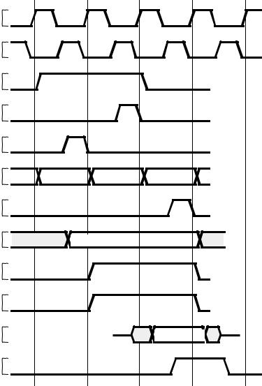
The remaining instructions to be considered are the load and store instructions. These all take three cycles to execute, since a bus transaction is required to transfer the data to or from the memory. For long displacement loads and stores, the displacement has been previously fetched into the displacement register. For the quick forms, the immediate displacement in the instruction word is used.
Figure7-34 shows the timing for execution of load and quick load instructions. The base address register is read from register file port1 and enabled onto the op1 bus. For long displacement loads, the previously fetched displacement is enabled onto the op2 bus, and for quick loads, the sign extended immediate displacement is enabled onto the op2 bus. The ALU function code is set to add, to form the effective address on the result bus, and this is latched into the memory bus address register during the second half of the first execute cycle. During the next two cycles the controller performs a memory read transaction, with the fetch signal held negated. The data from the data bus is enabled onto the result bus through the connecting buffer, and latched into the register result latch. This value is then written back to the register file during the first cycle of the subsequent instruction fetch.

7. Sample Models: The DP32 Processor |
7-55 |
phi1
phi2
reg_port1_en
disp_out_en or immed_ signext_en
ALU_op
addr_latch_en
dr_en
reg_res_ latch_en
reg_port3_en
a_bus
fetch
read
d_bus
ready
execute_0 |
execute_1 |
execute_2 |
fetch_0 |
add |
disable |
|
|
load address |
|
|
|
|
|
valid data in |
|
Figure7-34. Execution of load instructions.
7-56 |
The VHDL Cookbook |
The timing for execution of store and quick store instructions is shown in Figure7-35. As with load instructions, the base address and displacement are added, and the effective address is latched in the memory bus address register. During the next two cycles the controller performs a bus write transaction. The multiplexor for the register file port2 address is set to select the r3 field of the instruction, which specifies the register to be stored, and the port2 output is enabled onto the op2 bus. The buffer between the op2 bus and the memory data bus is enabled to transmit the data to the memory. Execution of the instruction completes at the end of the bus transaction.
Returning to the VHDL description, the first cycle of execution of load and store instructions is included as a branch of the nested case in the execute_0 state. The base address register output port is enabled, and either the displacement latch output or the sign extension buffer is enabled, depending on the instruction type. The ALU function code is set to add the two to form the effective address. The process then waits until phi2 changes to '1', indicating the second half of the cycle, and pulses the address latch enable. The next state is then set to execute_1 to continue execution of the instruction.
In state execute_1, the process firstly removes the base address, displacement and effective address from the DP32 internal buses, then starts a memory bus transaction. For load instructions, the fetch signal is negated and the read signal is asserted. For store instructions, the source register value is enabled onto the op2 bus, the memory data bus output buffer is enabled, and the write signal is aserted. The next state variable is then set to execute_2 for the next cycle.
In state execute_2, for load instructions, the memory data bus input buffer is enabled to transmit the data onto the result bus. The process then waits until phi2 is '1', in the second half of the cycle, and pulses the enable for the register result latch. The write back pending flag is then set to schedule the destination register write during the next instruction fetch cycle. For both load and store instructions, the next state is fetch_0. All control signals set during the execute_1 state will be returned to their negated values in the fetch_0 state.
The test bench described in Section7.5 can be used to test the register transfer architecture of the DP32. This is done using an alternate configuration, replacing the behavioural architecture in the test bench with the register transfer architecture. Figure7-36 shows such a configuration. The entity bindings for the clock generator and memory are the same, using the behavioural architectures, but the processor component instance uses the rtl architecture of the dp32 entity. This binding indication is followed by a configuration for that architecture, binding the entities described in Sections7.6.1–7.6.9 to the component instances contained in the architecture. The newly configured description can be simulated using the same test programs as before, and the results compared to verify that they implement the same behaviour.

7. Sample Models: The DP32 Processor |
7-57 |
phi1
phi2
reg_port1_en
disp_out_en or immed_ signext_en
ALU_op
addr_latch_en
reg_port2_ mux_sel
reg_port2_en
d2_en
a_bus
fetch
read
write
d_bus
ready
execute_0 execute_1 execute_2 |
|
add |
disable |
|
store address |
|
valid data out |
Figure7-35. Execution of store instructions.
7-58 |
The VHDL Cookbook |
use work.dp32_types.all;
configuration dp32_rtl_test of dp32_test is
for structure
for cg : clock_gen
use entity work.clock_gen(behaviour) generic map (Tpw => 8 ns, Tps => 2 ns);
end for;
for mem : memory
use entity work.memory(behaviour); end for;
for proc : dp32
use entity work.dp32(rtl); for rtl
for all : reg_file_32_rrw
use entity work.reg_file_32_rrw(behaviour); end for;
for all : mux2
use entity work.mux2(behaviour); end for;
for all : latch
use entity work.latch(behaviour); end for;
for all : PC_reg
use entity work.PC_reg(behaviour); end for;
for all : ALU_32
use entity work.ALU_32(behaviour); end for;
for all : cond_code_comparator
use entity work.cond_code_comparator(behaviour); end for;
for all : buffer_32
use entity work.buffer_32(behaviour); end for;
for all : latch_buffer_32
use entity work.latch_buffer_32(behaviour); end for;
for all : signext_8_32
use entity work.signext_8_32(behaviour); end for;
end for; end for;
end for;
end dp32_rtl_test;
Figure7-36. Configuration using register transfer architecture of DP32.