

Allen and Holberg - CMOS Analog Circuit Design
.pdfAllen and Holberg - CMOS Analog Circuit Design |
Page V.1-7 |
EXAMPLES
1.What is the on resistance of an enhancement MOS switch if VS = 0V, VG = 10V, W/L = 1, VTO = 1V, and K' = 25µA/V2?
Assume that vDS ≈ 0V. Therefore,
RON ≈ |
vDS |
= |
L/W |
|
iD |
K'(VG-VS -VT) |
|||
|
|
|||
|
106 |
|
||
RON = |
25(10-1) = 4444Ω |
|||
2.If VG=10V at t=0, what is the W/L value necessary to discharge C1 to
with 5% of its intial charge at t=0.1µS? Assume K'=25µA/V2
and VTO = 1V. |
|
|
|
||||
|
v(t) |
= |
5exp(-t/RC) |
|
→ |
||
|
|
-7 |
|
|
|
10 |
-7 |
10 |
|
|
= 20 |
|
|
||
exp RC |
|
→ RC = ln(20) |
|||||
Therefore, R = 106 x 103Ω
VG
C2=10pF
+
5V+  - C1=20pF
-
Thus, |
10x103 |
L/W |
|
L/W |
||
|
6 |
= |
K'(VG-VS-VT) |
= |
(2.5x10⁻⁵)(9) |
|
Gives |
W |
= 2.67 |
|
|
|
|
L |
|
|
|
|||
Allen and Holberg - CMOS Analog Circuit Design |
Page V.1-8 |
INFLUENCE OF PARASITIC CAPACITANCES
MOSFET Model for Charge Feedthrough Analysis
Distributed Model
G
CGDO |
CGSO |
D |
S |
RCH |
CGC=Cox |
Simplified Distributed Model
|
G |
CGDO |
CGSO |
Cox |
Cox |
2 |
2 |
D |
S |
RCH
CGSO = Voltage independent (1st-order), gate-source, overlap cap. CGDO = Voltage independent (1st order), drain-source overlap cap. CGC = Gate-to-channel capacitance (Cox)
RCH = Distributed drain-to-source channel resistance
Allen and Holberg - CMOS Analog Circuit Design |
Page V.1-9 |
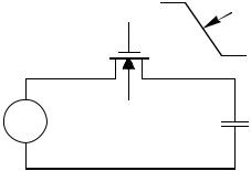
Charge Injection Sensitivity to Gate Signal Rate
Model:
vG |
dvG |
|
dt |
+ |
|
vIN |
CHold |
-
Case 1 - Slow Fall Time:
•Gate is inverted as vG goes negative .
•Channel time constant small enough so that the charge on CHold is absorbed
by vIN.
• When gate voltage reaches vIN+VT, the device turns off and feedthru occurs via the overlap capacitance.
Case 2 - Fast Fall Time:
•Gate is inverted as vG goes negative.
•Fall rate is faster than the channel time constant so that feedthru occurs via the channel capacitance onto CHold which is not absorbed by vIN.
•Feedthru continues when vG reaches vIN+VT.
•Total feedthru consists of that due to both the channel capacitance and the overlap capacitances.
Other Considerations:
•Source resistance effects the amount of charge shared between the drain and the source.
•The maximum gate voltage before negative transition effects the amount of charge injected.
Allen and Holberg - CMOS Analog Circuit Design |
Page V.1-10 |
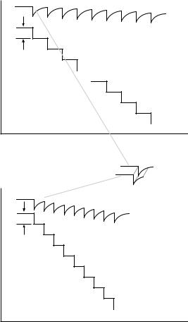
Intuition about Fast and Slow Regimes
To develop some intuition about the fast and slow cases, it is useful to model the gave voltage as a piecewise constant waveform (a quantized waveform) and consider the charge flow at each transition as illustrated below. In this figure, the range of voltage at CL illustrated represent the period while the transistor is on.
In both cases, the quantized voltage step is the same, but the time between steps is different. The voltage accross CL is observed to be an exponential whose time
constant is due to the channel resistance and channel capacitance and does not change from fast case to slow case.
vCL
V
Voltage  vGATE
vGATE
Time
(d)
V
Voltage
Time
(e)

Allen and Holberg - CMOS Analog Circuit Design |
Page V.1-11 |
Illustration of Parasitic Capacitances
φ1
|
CGS |
|
CGD |
|
+ |
|
VSS |
|
+vC1 |
|
|
|
||
V |
C |
C |
C |
|
BS |
BD |
1 |
|
|
IN |
|
|
|
- |
- |
|
|
|
|
|
|
|
|
CGS and CGD result in clock feedthrough
CBS and CBD cause loading on the desired capacitances
Clock Feedthrough
Assume slow fall and rise times
φ1
Switch ON
|
φ1 Switch OFF |
|
φ1 |
|
CGS |
+ |
VSS |
|
|
VIN |
CBS |
-
Clock signal couples through CGD on the rising part of signal when switch is off, but
V charges C1 to the right value regardless.
IN
Clock signal couples through CGD CGD on the falling part of the  signal when the switch is off.
C1 +vC1
-
vC1 |
|
CGD |
|
Δφ1 |
CGD |
Δφ1 |
CGD |
||
= - |
|
|
≈ - |
|
= - |
(vin + VT) |
|||
|
C1+CGD |
|
|
C1 |
|
|
C1 |
||
Allen and Holberg - CMOS Analog Circuit Design Page V.1-12
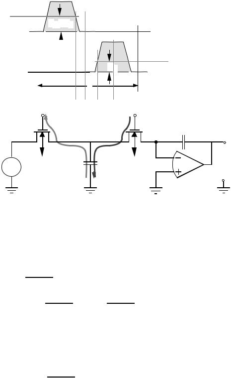
EXAMPLE - Switched |
Capacitor |
Integrator (slow clock edge |
|
regime) |
|
|
|
φ |
|
|
|
Switch ON |
|
|
|
Switch OFF vIN+VT |
|
|
|
|
|
|
Switch ON |
|
VT |
|
Switch OFF |
|
T |
|
|
φ |
t1 t 2 t 3 t 4 |
φ2 |
|
1 |
|
|
|
M1 |
|
|
C2 |
|
|
M2 |
|
+ |
|
|
+ |
|
|
|
|
V |
C |
VSS |
vOUT |
SS |
|
||
VIN |
1 |
|
|
|
|
|
|
- |
- |
|
assuming: CGS1=CGS2=CGD1=CGD2 = CG
Net feedthrough on C1 at t2:
|
CG |
|
|
|
|
|
|
VC1 = − CG+C1 (VIN + VT) |
|
|
|
||||
|
|
CG |
|
|
|
CG |
|
VC1 = VIN |
1 − |
C +C |
|
−VT |
C +C |
|
|
|
|
1 |
G |
|
|
G |
1 |
At t3, additional charge has been added due to CGS overlap of M2 as φ2 goes positive. Note that M2 has not turned on yet.
CG
VC1 (t2-t3) = CG+C1 VT
Allen and Holberg - CMOS Analog Circuit Design |
Page V.1-13 |
Giving at the end of t3 (before M2 turns on):
|
|
CG |
|
VC1 |
= VIN 1−C +C |
|
|
|
|
1 |
G |
+
Once M2 turns on (at t3 ), all of the charge on C1 is transferred to C2.
C1 |
C1 |
− |
CG |
|
VO = −VC1 |
= −VIN 1 |
|
|
|
C2 |
C2 |
|
C1+CG |
|
+
Between times at t3 and t4 additional charge is transferred to C1 from the channel capacitance of M2.
|
|
Cch |
|
|
|
|
|
VO (t3-t4)= − C2 (Vclk −VT) |
|
||||||
The final change in Vout is: |
|
|
|
|
|
||
C1 |
CG |
|
− |
Cch |
|
||
VO = −VIN |
1− |
|
|
|
(Vclk − VT) |
||
C2 |
C1+CG |
|
|
C2 |
|
||
|
|
|
|
|
|
C1 |
|
Ideally the output voltage change is −VIN C2 so the error due to charge |
|||||||
feedthrough is: |
|
|
|
|
|
|
|
VO (error) = |
C1 CG |
|
|
Cch |
|||
VIN |
|
|
|
|
− |
(Vclk − VT) |
|
|
C2 C1+CG |
|
C2 |
|
|||

Allen and Holberg - CMOS Analog Circuit Design |
Page V.1-14 |
Rigorous Quantitative Analysis of Fast and Slow Regimes
Consider the gate voltage traversing from VH to VL (e.g., 5.0 volts to 0.0 volts, respectively) described in the time domain as
vG = VH − Ut |
(3) |
When operating in the slow regime defined by the relationship
β V 2
HT >> U
2CL
where VHT is defined as
VHT = VH − VS − VT
the error (the difference between the desired voltage VS VCL) due to charge injection can be described as
(4)
(5)
and the actual voltage,

Allen and Holberg - CMOS Analog Circuit Design Page V.1-15
|
|
C c h |
|
|
|
|
|
|
|
|
|
|
|
|
|
|
|
||
W · C G D 0 + |
2 |
π U CL + W · C G D 0 (VS + VT − VL ) |
|
||||||
Verror = |
CL |
|
|
(6) |
|||||
|
|
|
|
2β |
|
CL |
|
||
In the fast swithing regime defined by the relationship |
|
||||||||
β V HT2 |
<< U |
|
|
|
|
|
|
(7) |
|
2CL |
|
|
|
|
|
|
|
||
|
|
|
|
|
|
|
|
|
|
the error voltage is given in Eq. (8) below as |
|
|
|||||||
|
|
Cch |
|
|
|
|
|
|
|
W·CGD0 + |
|
|
|
β |
3 |
|
|
||
2 |
|
|
W·CGD0 |
|
|||||
Verror = |
|
|
|
− |
VHT |
|
|||
CL |
|
V H T |
|
+ |
(VS + VT − VL ) |
(8) |
|||
|
|
|
|
|
6U CL |
CL |
|
||
The following example illustrates the application of the charge-feedthrough model given by Eq’s. (3) through (8).
Example 4.1-1 Calculation of charge feedthrough error
Calculate the effect of charge feedthrough on the circuit shown in Fig. 4.1-9 where Vs = 1.0 volts, CL = 200 fF, W/L = 0.8 m/0.8 m, and VG is given for two cases illustrated below. Use model parameters from Tables 3.1-2 and 3.2-1. Neglect L and W effects.
5 |
Case 2 |
vG |
Case 1 |
0 |
 0.2 ns
10 ns
Time
Case 1:
The first step is to determine the value of U in the expression vG = VH - Ut
For a transition from 5 volts to 0 volts in 0.2 ns, U = 25 109
In order to determine operating regime, the following relationship must be tested.
Allen and Holberg - CMOS Analog Circuit Design |
|
|
Page V.1-16 |
||||||||
|
β V 2 |
|
|
|
|
β V |
2 |
|
|
|
|
|
HT |
>> U for slow |
or |
|
HT |
<< U for fast |
|
||||
|
2CL |
2CL |
|
||||||||
|
|
|
|
|
|
|
|
|
|||
Observin g that there is a backbias on the transistor switch effecting VT, VHT is |
|||||||||||
giving |
VHT = VH - VS - VT = 5 - 1 - 0.887 = 3.113 |
|
|
|
|||||||
β VHT2 |
|
|
|
|
|
|
|
|
|
|
|
|
= |
110×10-6× 3.1132 |
2.66 × 10⁹ << 25 × 109 thus fast regime. |
||||||||
|
2CL |
|
2 × 200f |
|
= |
||||||
|
|
|
|
|
|
|
|
|
|
||
Applying Eq. (8) for the fast regime yields |
|
|
|
|
|||||||
|
|
|
|
1.58×10⁻¹⁵ |
|
3.32×10⁻³ |
176×10-18 |
|
|||
Verror |
176×10-18 + |
2 |
|
|
|
|
|||||
= |
|
200×10-15 |
|
3.113 - |
+ |
200×10-15 |
(5 + 0.887 - 0) |
||||
|
|
|
|
|
|
30×10-3 |
|
|
|||
Verror = 19.7 mV
Case 2:
The first step is to determine the value of U in the expression
v G = VH - Ut
For a transition from 5 volts to 0 volts in 10 ns, U = 5 × 10⁸ thus indicating the slow regime according to the following test
2.66 × 10⁹ >> 5 × 10⁸
|
|
1.58×10⁻¹⁵ |
314×10-6 |
|
176×10-18 |
|
|
176×10-18 + |
2 |
|
|
|
|||
Verror = |
200×10-15 |
|
220×10-6 |
+ |
200×10-15 |
(5 + 0.887 - 0 ) |
|
|
|
|
|
||||
Verror = 10.95 mV