

Allen and Holberg - CMOS Analog Circuit Design
.pdfAllen and Holberg - CMOS Analog Circuit Design |
Page I.3-4 |
BIPOLAR VS. MOS TRANSISTORS
CATEGORY |
BIPOLAR |
CMOS |
Turn-on Voltage |
0.5-0.6 V |
0.8-1 V |
Saturation Voltage |
0.2-0.3 V |
0.2-0.8 V |
gm at 100 A |
4 mS |
0.4 mS (W=10L) |
Analog Switch |
Offsets, asymmetric |
Good |
Implementation |
|
|
Power Dissipation |
Moderate to high |
Low but can be large |
Speed |
Faster |
Fast |
Compatible Capacitors |
Voltage dependent |
Good |
AC Performance |
DC variables only |
DC variables and |
Dependence |
|
geometry |
Number of Terminals |
3 |
4 |
Noise (1/f) |
Good |
Poor |
Noise Thermal |
OK |
OK |
Offset Voltage |
< 1 mV |
5-10 mV |
Allen and Holberg - CMOS Analog Circuit Design |
Page I.3-5 |
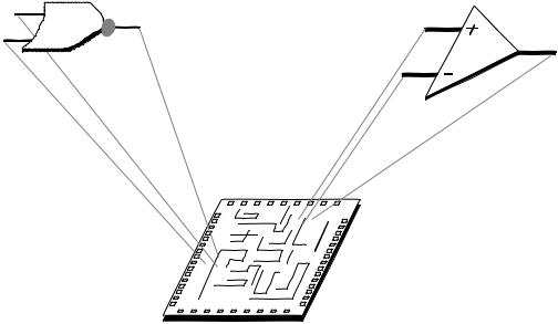
WHY CMOS???
CMOS is nearly ideal for mixed-signal designs:
•Dense digital logic
•High-performance analog
DIGITAL |
ANALOG |
MIXED-SIGNAL IC
Allen and Holberg - CMOS Analog Circuit Design |
Page I.4-1 |
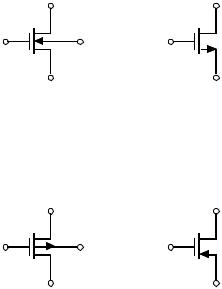
I.4 NOTATION
SYMBOLS FOR TRANSISTORS
Drain |
|
Drain |
Gate |
Bulk |
Gate |
Source |
|
Source/bulk |
n-channel, enhance- n-channel, enhance- |
||
ment, VBS ≠ 0 |
|
ment, bulk at most |
|
|
negative supply |
Drain |
|
Drain |
Gate |
Bulk |
Gate |
Source |
|
Source/bulk |
p-channel, enhance- p-channel, enhance- |
||
ment, VBS ≠ 0 |
|
ment, bulk at most |
|
|
positive supply |

Allen and Holberg - CMOS Analog Circuit Design |
Page I.4-2 |
SYMBOLS FOR CIRCUIT ELEMENTS
Operational Amplifier/Amplifier/OTA
+
 -
-
V I
+ |
+ |
A V |
GmV1 |
v 1 |
|
V1 |
V1 |
- |
- |
VCVS |
VCCS |
I1 |
I1 |
Rm I 1 |
Ai I1 |
CCVS |
CCCS |
Allen and Holberg - CMOS Analog Circuit Design |
Page I.4-3 |
Notation for signals
 Id
Id
 i d
i d 
ID
i D
time
Allen and Holberg - CMOS Analog Circuit Design |
Page II.0-1 |
II. CMOS TECHNOLOGY
Contents
II.1 |
Basic Fabrication Processes |
II.2 |
CMOS Technology |
II.3 |
PN Junction |
II.4 |
MOS Transistor |
II.5 |
Passive Components |
II.6 |
Latchup Protection |
II.7 |
ESD Protection |
II.8 |
Geometrical Considerations |
Allen and Holberg - CMOS Analog Circuit Design |
Page II.0-2 |
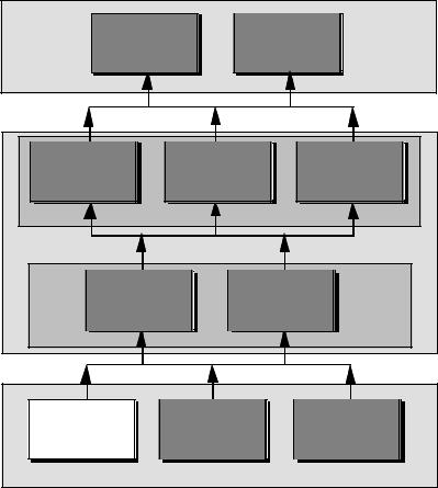
Perspective
Chapter 10
D/A and A/D
Chapter 11
Converters
Analog Systems
SYSTEMS |
|
|
Chapter 7 |
Chapter 8 |
Chapter 9 |
CMOS |
Simple CMOS |
High Performance |
Comparators |
Opamps |
Opamps |
COMPLEX |
|
|
CIRCUITS |
|
|
Chapter 5 |
|
Chapter 6 |
CMOS |
|
CMOS |
Subcircuits |
Amplifiers |
|
SIMPLE |
|
|
Chapter 2 |
Chapter 3 |
Chapter 4 |
CMOS |
CMOS Device |
Device |
Technology |
Modeling |
Characterization |
DEVICES |
|
|
Allen and Holberg - CMOS Analog Circuit Design |
Page II.0-3 |
OBJECTIVE
•Provide an understanding of CMOS technology sufficient to enhance circuit design.
•Characterize passive components compatible with basic technologies.
•Provide a background for modeling at the circuit level.
•Understand the limits and constraints introduced by technology.

Allen and Holberg - CMOS Analog Circuit Design |
Page II.1-1 |
II.1 - BASIC FABRICATION PROCESSES
BASIC FABRTICATION PROCESSES
Basic Steps
•Oxide growth
•Thermal diffusion
•Ion implantation
•Deposition
•Etching Photolithography
Means by which the above steps are applied to selected areas of the silicon wafer.
Silicon wafer
0.5-0.8 mm
125-200 mm
n-type: 3-5 Ω -cm p-type: 14-16 Ω -cm

Allen and Holberg - CMOS Analog Circuit Design |
Page II.1-2 |
Oxidation
The process of growing a layer of silicon dioxide (SiO2)on the surface of a silicon wafer.
Original Si surface |
tox |
SiO 2
0.44 tox |
Si substrate |
|
Uses:
•Provide isolation between two layers
•Protect underlying material from contamination
•Very thin oxides (100 to 1000 Å) are grown using dry-oxidation techniques. Thicker oxides (>1000 Å) are grown using wet oxidation techniques.