


Chapter 10: EISA System Buses
Chapter 10
The Previous Chapter
In the previous chapter, automatic system configuration was described.
This Chapter
This chapter describes the major buses found in virtually all EISA systems. This includes the host, EISA, ISA and X-buses.
The Next Chapter
The next chapter, “Bridge, Translator, Pathfinder, Toolbox,” describes the major functions provided by the EISA chipset.
Introduction
Refer to figure 10-1. EISA systems may incorporate a number of buses such as:
•Host bus
•EISA bus
•X-bus
•Local bus
117

EISA System Architecture
CPU |
Local Bus |
Cache |
Host Bus |
|
|
|
|
System
Memory
EISA Bus Buffers
EISA Bus
X-Bus Buffers
X-Bus
Figure 10-1. Buses Typically Found in EISA Systems
Host Bus
Virtually all EISA systems are shipped with an integral CPU. This CPU may be integrated onto the system board itself or may reside on a special, CPU daughter card that installs in a special connector on the system board. This is referred to as the host CPU. The host CPU's local address, data and control buses comprise the host bus. Typically, devices that the CPU requires fast access to would be placed on the host bus. These would include devices like:
•system board RAM memory
•numeric coprocessor
•local cache controller and cache memory
•non-cacheable access, or NCA, logic
118

Chapter 10: EISA System Buses
•advanced video controller
•other I/O devices requiring fast access to the CPU
If the host CPU resides on a daughter card, the CPU's local cache controller, cache memory, NCA logic and numeric coprocessor also typically reside on the CPU card.
EISA/ISA Bus
Since the ISA bus is a subset of the EISA bus, any reference to the EISA bus in this book is a reference to the ISA bus and its EISA extensions. The ISA bus is discussed in detail in the MindShare book entitled ISA System Architecture. The EISA extensions to the ISA bus are described earlier in this book.
X-Bus
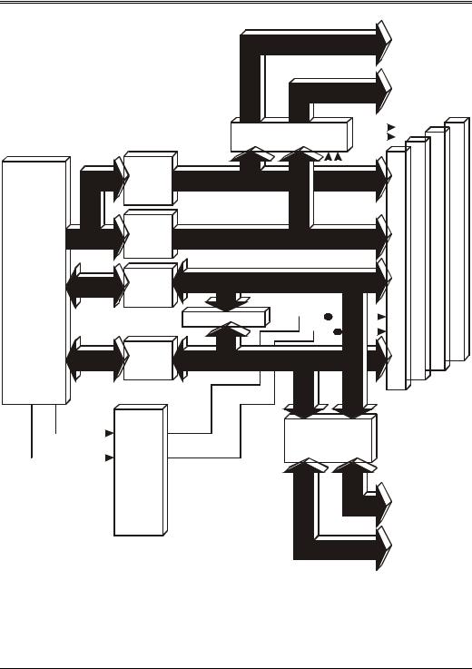
The ability of the microprocessor to drive data onto the data bus and the address onto the address bus is limited by the power of its output drivers. When the microprocessor is writing data to any external memory or I/O device, the data is driven out onto the processor's local data bus. If the local data bus is fanned out and connected to too many external devices, the drive capability of the microprocessor's output drivers may be exceeded and the data driven onto the data bus becomes corrupted. The local data bus is connected to the external data bus transceivers pictured in figure 10-2.
During a write operation, the bus control logic allows the appropriate data bus transceiver to pass data from the processor's local data bus onto the system data (SD) bus. The output drive capability of the transceiver is substantially greater than that of the processor's internal drivers, allowing the SD bus to fan out to more places. The SD bus is connected to all of the ISA expansion slots. In addition, many devices that may be written to are physically located on the system board itself. However, it would exceed the output drive capability of the data bus transceivers to fan out the SD bus to all of the devices integrated onto the system board as well as to all of the expansion slots.
To solve this problem, the SD bus is passed through another transceiver onto the XD, or extended data, bus. The X data bus transceiver redrives the data onto the XD bus during writes, permitting the data to be fanned out the devices residing on the XD bus. The devices integrated onto the system board are connected to the X data bus.
119
EISA System Architecture
|
|
|
|
|
|
|
|
|
|
|
|
|
XA17:XA23 |
||||||||||||
|
|
|
|
|
|
|
|
|
|
|
|
|
XA1:XA16 |
||||||||||||
|
|
|
|
|
|
|
|
|
|
|
|
|
|
|
|
|
XBHE# |
|
|
||||||
|
|
|
|
|
|
|
|
|
|
|
XA |
|
|
|
|
|
|||||||||
|
|
|
|
|
|
|
|
|
|
|
|
|
|
|
XA0 |
|
|
|
|
||||||
|
|
|
|
|
|
|
|
|
|
|
|
|
|
|
|
||||||||||
|
|
|
|
|
|
|
|
|
|
Bus Buffer |
|
|
|
|
|
|
|
|
|
||||||
|
|
|
|
|
|
|
|
|
|
|
|
|
|
|
|
|
|
|
|||||||
|
|
|
|
|
|
|
|
|
|
|
|
|
|
|
|
|
|
|
|
|
|
|
|
|
|
|
|
|
|
|
|
|
|
|
|
|
|
|
|
|
|
|
|
|
|
|
|
|
|
|
|
|
|
|
|
|
LA |
|
|
|
|
|
|
|
|
|
|
|
|
|
|
|
|
|
|
|
|
|
|
|
|
|
|
|
|
|
|
|
|
|
|
|
|
|
|
|
|
|
|
|
|
|
|
|
|
|
|
|
Bus |
|
|
LA17:LA23 |
|
|
|
|
|
|
|
|
|
|
|
|
|
|
|
|
|
|
|
|
|
|
Buffer |
|
|
|
|
|
|
|
|
|
|
|
|
|
|
|
|
|
|
|
|
CPU |
|
|
|
|
|
|
|
|
|
|
|
|
|
|
|
|
|
|
|
|
|
|
|
||
|
|
|
|
|
|
|
|
|
|
|
|
|
|
|
|
|
|
|
|
|
|
|
|||
|
|
Address |
|
|
|
|
|
|
|
|
|
|
|
|
|
|
|
|
|
|
|
|
|||
|
|
|
|
|
|
|
|
|
|
|
|
|
|
|
|
|
|
|
|
|
|
|
|
|
|
|
|
|
A1:A23 |
Latch |
|
|
SA1:SA19 |
|
|
|
|
|
|
|
|
|
|
|
|
|
|
|
|
||
|
|
|
|
|
|
|
|
|
|
|
|
|
|
|
|
|
|
|
|
|
|
|
|
|
|
|
|
|
|
|
|
|
|
|
|
|
|
|
|
|
|
|
|
|
|
|
|
|
|
|
|
|
|
|
|
|
Data |
|
|
|
SD8:SD15 |
|
|
|
|
|
|
|
|
|
|
|
|
|
|||
|
|
|
D8:D15 |
Bus |
|
|
|
|
|
|
|
|
|
|
|
|
|
|
|
|
|||||
|
|
|
|
|
Xcvr |
|
|
|
|
|
|
|
|
|
|
|
|
|
|
|
|
|
|
|
|
|
|
|
|
|
|
|
|
|
|
|
|
|
|
|
|
|
|
|
|
|
|
|
|
|
|
|
|
|
|
|
|
|
|
Hi/Lo Copier |
|
|
|
|
|
|
|
|
|
|
|
|
|
|
|
|
|
|
|
|
|
|
|
|
|
|
|
|
|
|
|
|
|
|
|
|
|
|
|
||||
|
|
|
|
|
|
|
|
|
|
|
|
|
|
|
|
|
|
|
|
|
|
|
|
|
|
|
|
|
|
|
|
|
|
|
|
|
|
|
|
|
|
|
|
|
|
|
|
|
|
|
|
|
|
|
|
|
Data |
|
|
|
|
|
|
|
|
|
|
|
|
|
|
|
|
|
|
|
|
|
|
|
D0:D7 |
Bus |
|
|
|
SD0:SD7 |
|
|
|
|
|
|
|
|
|
|
|
|
|
||||
|
|
|
|
|
|
|
|
|
|
|
|
|
|
|
|
|
|
|
|||||||
|
|
|
|
|
Xcvr |
|
|
|
|
|
|
|
|
|
|
|
|
|
|
|
|
|
|
|
|
|
|
|
|
|
|
|
|
|
|
|
|
|
|
|
|
|
|
|
|
|
|
|
|
|
|
|
|
|
|
|
|
|
|
|
|
|
|
|
|
|
|
|
|
|
|
|
|
Expansion |
|||
|
|
|
|
|
|
|
|
|
|
|
|
|
|
|
|
|
|
|
|
|
|
||||
|
|
|
|
|
|
|
|
|
|
|
|
|
|
|
|
|
|
|
|
|
|
|
Slots |
||
|
|
|
A0 |
|
|
SA0 |
|
|
|
|
|
|
|
|
|
|
|
|
|
|
|
|
|||
|
|
|
|
|
|
|
|
|
XD |
|
|
|
|
|
|
|
|
||||||||
|
|
|
|
|
|
|
|
|
|
|
|
|
|
|
|
|
|
|
|
|
|
||||
|
|
BHE# |
|
SBHE# |
|
|
Bus Buffer |
|
|
|
|
|
|
|
|||||||||||
|
|
|
|
|
|
|
|
|
|
|
|
|
|
|
|
|
|
|
|||||||
|
|
|
|
|
|
|
|
|
|
|
|
|
|
|
|
|
|
|
|
|
|
|
|
|
|
Bus |
|
Control |
|
logic |
XD8:15 |
|
|
|
XD0:XD7 |
Figure 10-2. The X-Bus
120

Chapter 10: EISA System Buses
When a write is in progress, the bus control logic sets up the data bus transceivers to pass data from the microprocessor's local data bus onto the SD bus and also enables the X data bus transceiver to pass data from the SD bus to the XD bus. When a read is in progress, the bus control logic sets up the X data bus transceiver to pass data from the XD to the SD bus and sets up the data bus transceivers to pass data from the SD to the microprocessor's local data bus. It should be noted that the XD bus is just a buffered version of the ISA bus's SD bus.
The same fanout problem exists on the processor's address bus. The address generated by the microprocessor is driven onto the processor's local address bus. In an ISA machine, it then passes through the LA bus buffer, the address latch and the bus control logic onto the ISA address bus. The ISA address bus consists of LA[23:17], SA[19:0] and SBHE#. The redrive capability of the LA bus buffer, the address latch and the bus control logic permits the address information to be fanned out to all of the ISA expansion slots. In addition to the ISA devices installed in expansion slots, however, the address information must also be fanned out to the addressable devices that are integrated onto the system board. This would exceed the drive capability of the LA bus buffer, the address latch and the bus control logic. To allow additional fanout, the ISA address information is passed through a buffer onto the XA bus. The buffer's redrive capability permits the XA address to be fanned out to all the devices integrated onto the system board. In other words, the devices integrated onto the system board are connected to the XA and XD buses, a buffered version of the ISA address bus.
121

EISA System Architecture
122