


Functional Overview
2.1.4DMA ports
The DMA ports are optional. They permit high-bandwidth peripherals direct access to the PrimeCell VC-SDRAM Controller without data having to pass over the main system bus. The control engine prioritizes accesses and can hide the following DRAM commands:
•bank activate
•restore
•prefetch.
With a single bus interface, data transfer to the PrimeCell VC-SDRAM Controller, can be halted whenever an access is requested to an address which is not available in a virtual channel. With multiple bus interfaces, the halted time on one bus can be used to permit data transfer to another bus if its requested data is in a virtual channel.
The exact requirement for each DMA port is application specific.
As with the bus interface, channels can be locked so that only accesses sourced from the DMA ports are able to re-allocate them.
DMA accesses to the PrimeCell VC-SDRAM Controller are quad word. For slow, low-bandwidth DMA peripherals, data can be buffered into quad words before it is written to the PrimeCell VC-SDRAM Controller, so that most efficient use of the quad word bursts is maintained.
2.1.5Pad interface
All data and control signals must be passed synchronously to the VC-SDRAMs. Resynchronization from the ASIC clock domain to the external bus clock domain is achieved in this block. The external bus clock can either be fed back from the external clock (using a tristate pad), and used directly, or fed into a PLL so the phase of the external clock is fixed relative to the on-chip clock.
2-6 |
© Copyright ARM Limited 1999. All rights reserved. |
ARM DDI 0162B |
Functional Overview
2.2Overview of a VC-SDRAM, ASIC/ASSP, unified memory system
Figure 2-2 shows the PrimeCell VC-SDRAM Controller interfacing VC-SDRAM chips to SoC ASIC peripherals.
ASIC/ASSP |
|
|
|
|
|
|
Bus |
System |
|
|
|
|
|
peripheral |
controller |
|
|
|
|
|
|
On-chip |
|
|
|
|
|
ARM |
system bus |
AHB bus |
|
|
|
|
|
|
|
|
VC-SDRAM |
||
processor |
|
|
|
|
||
|
interface |
|
|
D[15:0] |
||
|
|
|
|
|||
|
|
|
|
|
||
High-speed DMA |
DMA bus 2 |
|
|
A[13:0] |
|
|
|
peripheral 2 |
|
PrimeCell |
|
|
|
|
|
|
|
|
||
|
|
|
|
|
|
|
|
|
|
VCPrimeCell-SDRAM |
Pad |
|
|
|
|
|
VCcontroller-SDRAM |
Control |
|
|
|
|
|
interface |
|
||
High-speed DMA |
DMA bus 1 |
controller |
|
|||
|
|
|||||
|
|
|
||||
|
peripheral 1 |
|
|
|
|
|
|
|
|
|
|
D[31:16] |
|
High-speed DMA |
DMA bus 0 |
|
|
External |
VC-SDRAM |
|
|
peripheral 0 |
|
|
|
|
|
|
|
|
|
clock |
|
|
|
|
|
|
|
|
|
|
|
Internal clock domain |
domain |
|
||
|
|
|
|
|||
Figure 2-2 PrimeCell VC-SDRAM Controller in a system
The system uses three types of bus:
•External bus
•Internal bus
•DMA bus on page 2-8 (optional).
2.2.1External bus
The off-chip VC-SDRAM bus (containing data, address and control signals) connects the ASIC or ASSP to the VC-SDRAM.
2.2.2Internal bus
The on-chip bus enables communication between the on-chip peripherals. The PrimeCell VC-SDRAM Controller appears as a standard slave on the on-chip bus and controls the VC-SDRAM on the external bus.
ARM DDI 0162B |
© Copyright ARM Limited 1999. All rights reserved. |
2-7 |

Functional Overview
2.2.3DMA bus
To improve system performance, up to three DMA buses can also be interfaced to the PrimeCell VC-SDRAM. The DMA channels permit multiple access requests to be presented to the controller at the same time. This enables it to hide many of the background operations (for example, bank activate, channel prefetch, and restore operations), and thus reduce the average system access latency.
Multi-port access
Multi-port access to the PrimeCell VC-SDRAM Controller permits:
•higher memory bandwidth by hiding more of the non-data transfer operations
•potentially higher performance on the main AMBA bus by removing the heavy DMA traffic
•potentially less overall bus capacitance and therefore lower power consumption.
To permit maximum reuse flexibility the bus interface section has been separated from, and has a clean interface to, the PrimeCell VC-SDRAM control engine.
Clock domains
Figure 2-2 on page 2-7 shows that there are two clock domains in a synchronous memory system, on-chip and off-chip. The off-chip clock domain will be phase-shifted with respect to the on-chip clock domain due to the pad delays. The on-to-off chip clock skew requires careful attention at clock speeds greater than 80MHz, so the pad interface has been separated from the main PrimeCell VC-SDRAM control engine. The separation permits easy implementation of the most appropriate clock resynchronisation strategy taking into account interface speed and available pad library.
Maintaining memory during low-power sleep modes
In many systems, the contents of the memory system needs to be maintained during low-power sleep modes. To aid the design of this class of system, two features are provided in the PrimeCell VC-SDRAM Controller:
•VC-SDRAM refresh over soft reset
•a mechanism to place the VC-SDRAMs into self-refresh mode.
The above features enable interaction with a system controller, which will typically be present to control the safe transition between power-up, reset, normal, and sleep modes. The associated control signals can be tied off if not required.
2-8 |
© Copyright ARM Limited 1999. All rights reserved. |
ARM DDI 0162B |

Functional Overview
2.2.4Locking virtual channels to DMA and bus interface ports
With virtual channel memory, the bus and DMA interface ports can request virtual channels to be locked for their own use. This feature permits a guaranteed low-latency virtual channel access for DMA devices with linearly incrementing addresses.
Note
The above feature is not available for SDRAMs, which have no channels to lock.
All virtual channels can be read from, or written to, by any bus master requesting access on any of the four virtual channel interface ports. However locked virtual channels can only be re-allocated (that is, restored and prefetched) by the interface port to which they are locked. Channel re-allocation takes place when data required by an access is not present in a virtual channel (that is, a channel miss) and one of the 16 virtual channels (the replacement candidate) needs to be chosen to cache the data required to complete the access request.
To lock channels, the interface port sets the relevant lock bits in the vector Lockn[15:0], where n is the port number 0-3. Each bit in the vector Lockn represents virtual channel 15 – 0. If a port requesting access has channels locked to it, and an access request results in a channel miss, then only those locked channels will be considered as replacement candidates by the channel re-allocation system.
Note
If a port does not lock any channels to itself, then all channels except those locked by other ports will be considered as replacement candidates.
Channels locked to more than one port will be replacement candidates for each of the ports they are locked to.
Channels are locked to a DMA or bus interface port for data access types:
•read
•write
•prefetch.
Prefetch can be used to good effect with simple incrementing address DMA ports such as used for video display.
When the DMA port reads or writes data to the last address in a virtual channel, then the DMA port can speculatively prefetch the next section of memory into the locked virtual channel, thus ensuring a channel hit for the next DMA request.
ARM DDI 0162B |
© Copyright ARM Limited 1999. All rights reserved. |
2-9 |
Functional Overview
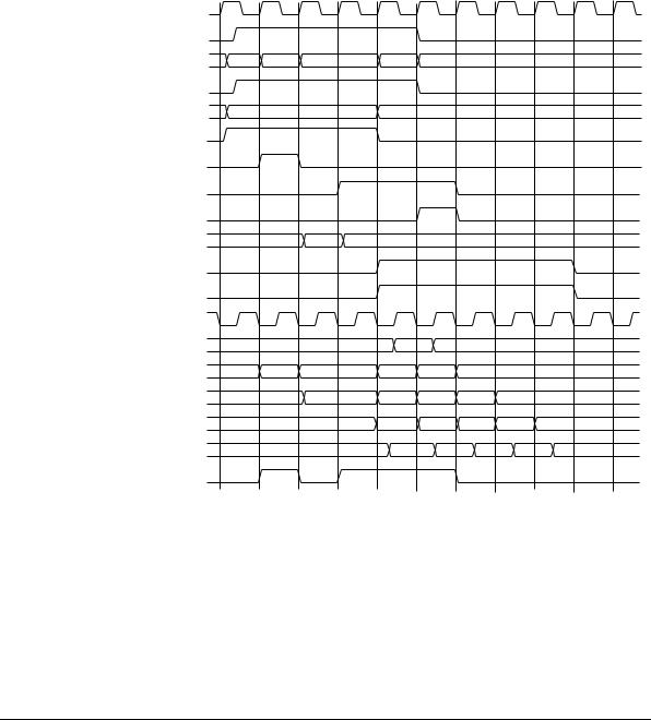
Figure 2-3 shows a PrimeCell VC-SDRAM Controller write example (merging write buffer off).
|
1 |
2 |
3 |
4 |
5 |
6 |
7 |
8 |
9 |
10 |
HCLK |
|
|
|
|
|
|
|
|
|
|
HSELram |
|
|
|
|
|
|
|
|
|
|
HADDR |
A0 |
A1 |
|
A2 |
A3 |
|
|
|
|
|
HWRITE |
|
|
|
|
|
|
|
|
|
|
Addrin3 |
|
|
A0 |
|
|
|
|
|
|
|
Write3 |
|
|
|
|
|
|
|
|
|
|
Write |
|
|
|
|
|
|
|
|
|
|
XferOut3 |
|
|
|
|
|
|
|
|
|
|
EndOfXfer3 |
|
|
|
|
|
|
|
|
|
|
Cmd |
|
|
WR |
|
|
|
|
|
|
|
ExtBusReq |
|
|
|
|
|
|
|
|
|
|
ExtBusGnt |
|
|
|
|
|
|
|
|
|
|
CLKIn |
|
|
|
|
|
|
|
|
|
|
VCSDRAMCmd |
|
|
|
|
WR |
|
|
|
|
|
HWDATA |
|
D0 |
|
D1 |
D2 |
D3 |
|
|
|
|
DATAIn3 |
|
|
|
D0 |
D1 |
D2 |
D3 |
|
|
|
VcWrData |
|
|
|
|
D0 |
D1 |
D2 |
D3 |
|
|
DATAOut |
|
|
|
|
D0 |
D1 |
D2 |
|
D3 |
|
HREADYout |
|
|
|
|
|
|
|
|
|
|
Figure 2-3 PrimeCell VC-SDRAM Controller write example
2-10 |
© Copyright ARM Limited 1999. All rights reserved. |
ARM DDI 0162B |
Functional Overview
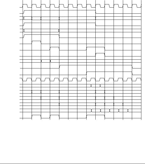
Figure 2-4 shows a second PrimeCell VC-SDRAM Controller write example (delayed
ExtBusGnt signal).
|
1 |
2 |
3 |
4 |
5 |
6 |
7 |
8 |
9 |
10 |
11 |
12 |
13 |
HCLK |
|
|
|
|
|
|
|
|
|
|
|
|
|
HSELram |
|
|
|
|
|
|
|
|
|
|
|
|
|
HADDR |
A0 |
A1 |
A2 |
|
|
|
A3 |
|
|
|
|
|
|
HWRITE |
|
|
|
|
|
|
|
|
|
|
|
|
|
Addrin3 |
|
|
A0 |
|
|
|
|
|
|
|
|
|
|
WRITE3 |
|
|
|
|
|
|
|
|
|
|
|
|
|
WRITE |
|
|
|
|
|
|
|
|
|
|
|
|
|
XferOut3 |
|
|
|
|
|
|
|
|
|
|
|
|
|
EndOfXfer3 |
|
|
|
|
|
|
|
|
|
|
|
|
|
Cmd |
|
|
WR |
|
|
|
|
|
|
|
|
|
|
ExtBusReq |
|
|
|
|
|
|
|
|
|
|
|
|
|
ExtBusGnt |
|
|
|
|
|
|
|
|
|
|
|
|
|
CLKIn |
|
|
|
|
|
|
|
|
|
|
|
|
|
VCSDRAMCmd |
|
|
|
|
|
|
|
WR |
|
|
|
|
|
HWDATA |
|
D0 |
D1 |
|
|
|
D2 |
|
D3 |
|
|
|
|
DATAIn3 |
|
|
D0 |
|
|
|
D1 |
|
D2 |
D3 |
|
|
|
VcWrData |
|
|
|
|
|
|
D0 |
|
D1 |
D2 |
D3 |
|
|
DATAOut |
|
|
|
|
|
|
|
D0 |
D1 |
D2 |
|
D3 |
|
HREADYout |
|
|
|
|
|
|
|
|
|
|
|
|
|
Figure 2-4 PrimeCell VC-SDRAM Controller write example
ARM DDI 0162B |
© Copyright ARM Limited 1999. All rights reserved. |
2-11 |

Functional Overview
Figure 2-5 shows a PrimeCell VC-SDRAM Controller read example.
|
1 |
2 |
3 |
4 |
5 |
6 |
7 |
8 |
9 |
10 |
11 |
12 |
13 |
14 |
HCLK |
|
|
|
|
|
|
|
|
|
|
|
|
|
|
HSELram |
|
|
|
|
|
|
|
|
|
|
|
|
|
|
HADDR |
A0 |
|
|
|
|
A1 |
|
|
|
A2 |
A3 |
|
|
|
HWRITE |
|
|
|
|
|
|
|
|
|
|
|
|
|
|
Addrin3 |
|
|
A0 |
|
|
|
|
|
|
|
|
|
|
|
READ3 |
|
|
|
|
|
|
|
|
|
|
|
|
|
|
READ |
|
|
|
|
|
|
|
|
|
|
|
|
|
|
XferOut3 |
|
|
|
|
|
|
|
|
|
|
|
|
|
|
EndOfXfer3 |
|
|
|
|
|
|
|
|
|
|
|
|
|
|
Cmd |
|
|
RD |
|
|
|
|
|
|
|
|
|
|
|
ExtBusReq
ExtBusGnt
CLKIn
VCSDRAMCmd |
RD |
|
|
|
|
|
VCSDRAMData |
D0 |
D1 |
D2 |
D3 |
|
|
(CL=3) |
|
|
|
|
|
|
VcRdData |
|
D0 |
D1 |
D2 |
D3 |
|
RdData |
|
|
D0 |
D1 |
D2 |
D3 |
RdData(Ahbif) |
|
|
D0 |
D1 |
D2 |
D3 |
|
|
|
||||
HRDATA |
|
|
D0 |
D1 |
D2 |
D3 |
HREADYout |
|
|
|
|
|
|
Figure 2-5 PrimeCell VC-SDRAM Controller read example
2-12 |
© Copyright ARM Limited 1999. All rights reserved. |
ARM DDI 0162B |