

PIC16F84A
4.0TIMER0 MODULE
The Timer0 module timer/counter has the following features:
•8-bit timer/counter
•Readable and writable
•Internal or external clock select
•Edge select for external clock
•8-bit software programmable prescaler
•Interrupt on overflow from FFh to 00h
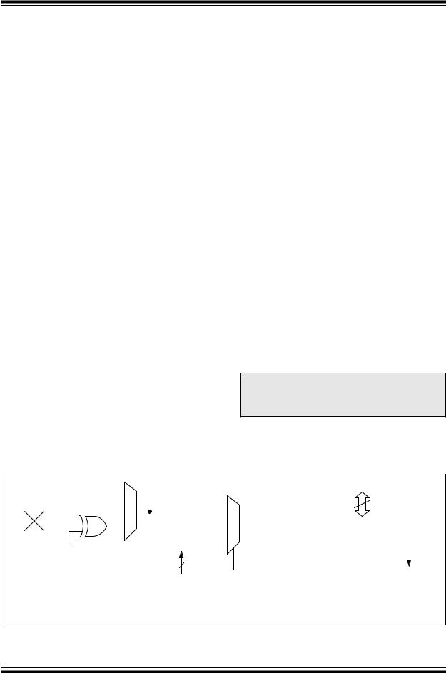
Figure 4-1 is a simplified block diagram of the Timer0 module.
Additional information on timer modules is available in the PICmicro™ Mid-Range Reference Manual, (DS33023).
4.1Timer0 Operation
Timer0 can operate as a timer or as a counter.
Timer mode is selected by clearing bit T0CS (OPTION_REG<5>). In timer mode, the Timer0 module will increment every instruction cycle (without prescaler). If the TMR0 register is written, the increment is inhibited for the following two instruction cycles. The user can work around this by writing an adjusted value to the TMR0 register.
Counter mode is selected by setting bit T0CS (OPTION_REG<5>). In counter mode, Timer0 will increment either on every rising or falling edge of pin RA4/T0CKI. The incrementing edge is determined by the Timer0 Source Edge Select bit T0SE (OPTION_REG<4>). Clearing bit T0SE selects the rising edge. Restrictions on the external clock input are discussed below.
When an external clock input is used for Timer0, it must meet certain requirements. The requirements ensure the external clock can be synchronized with the internal phase clock (TOSC). Also, there is a delay in the actual incrementing of Timer0 after synchronization.
Additional information on external clock requirements is available in the PICmicro™ Mid-Range Reference Manual, (DS33023).
4.2Prescaler
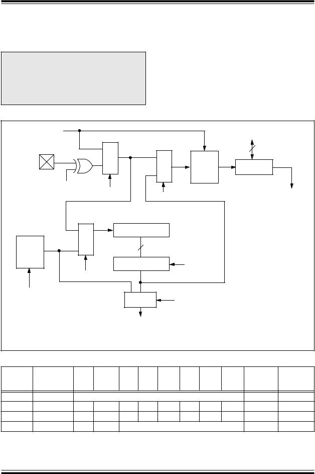
An 8-bit counter is available as a prescaler for the Timer0 module, or as a postscaler for the Watchdog Timer, respectively (Figure 4-2). For simplicity, this counter is being referred to as “prescaler” throughout this data sheet. Note that there is only one prescaler available which is mutually exclusively shared between the Timer0 module and the Watchdog Timer. Thus, a prescaler assignment for the Timer0 module means that there is no prescaler for the Watchdog Timer, and vice-versa.
The prescaler is not readable or writable.
The PSA and PS2:PS0 bits (OPTION_REG<3:0>) determine the prescaler assignment and prescale ratio.
Clearing bit PSA will assign the prescaler to the Timer0 module. When the prescaler is assigned to the Timer0 module, prescale values of 1:2, 1:4, ..., 1:256 are selectable.
Setting bit PSA will assign the prescaler to the Watchdog Timer (WDT). When the prescaler is assigned to the WDT, prescale values of 1:1, 1:2, ..., 1:128 are selectable.
When assigned to the Timer0 module, all instructions writing to the TMR0 register (e.g. CLRF 1, MOVWF 1, BSF 1,x....etc.) will clear the prescaler. When assigned to WDT, a CLRWDT instruction will clear the prescaler along with the WDT.
Note: Writing to TMR0 when the prescaler is assigned to Timer0 will clear the prescaler count, but will not change the prescaler assignment.
FIGURE 4-1: |
TIMER0 BLOCK DIAGRAM |
|
|
|
|
|
|
|
|||||||||||||
|
|
|
|
|
|
|
|
|
|
|
|
|
|
|
|
|
|
|
Data bus |
||
|
|
|
FOSC/4 |
|
|
0 |
|
|
|
|
|
1 |
PSout |
|
8 |
|
|
||||
|
|
|
|
|
|
|
|
||||||||||||||
|
|
|
|
|
|
|
|
|
|
|
|
|
|
|
|
|
|
||||
|
|
|
|
|
|
|
|
|
|
|
|
|
|
|
|
Sync with |
|
|
|
|
|
|
|
|
|
|
|
|
|
1 |
|
|
|
|
|
|
|
|
TMR0 |
|
|
||
|
|
|
|
|
|
|
|
|
|
|
|
|
|
Internal |
|
|
|
||||
|
|
|
|
|
|
|
|
|
|
|
|
|
|
|
|
|
clocks |
|
|
|
|
RA4/T0CKI |
|
|
|
|
|
|
|
|
|
Programmable |
|
|
0 |
|
|
PSout |
|
||||
pin |
|
|
|
|
|
|
|
|
|
Prescaler |
|
|
|
|
|
|
|
|
|||
T0SE |
|
|
|
|
|
|
|
|
|
|
(2 cycle delay) |
|
|
|
|
||||||
|
|
|
|
|
|
|
3 |
|
|
|
|
|
|
|
|
||||||
|
|
|
|
|
|
|
|
|
|
|
PSA |
|
|
Set interrupt |
|||||||
|
|
|
|
|
|
|
|
|
|
|
PS2, PS1, PS0 |
|
|
||||||||
|
|
|
|
|
|
|
|
|
|
|
|
|
flag bit T0IF |
||||||||
|
|
|
|
|
|
|
|
|
|
|
|||||||||||
|
|
|
|
|
|
T0CS |
|
|
|
|
on overflow |
||||||||||
Note 1: T0CS, T0SE, PSA, PS2:PS0 (OPTION_REG<5:0>).
2: The prescaler is shared with Watchdog Timer (refer to Figure 4-2 for detailed block diagram).
1998 Microchip Technology Inc. |
Preliminary |
DS35007A-page 17
PIC16F84A
4.2.1SWITCHING PRESCALER ASSIGNMENT
The prescaler assignment is fully under software control, i.e., it can be changed “on the fly” during program execution.
Note: To avoid an unintended device RESET, a specific instruction sequence (shown in the PICmicro™ Mid-Range Reference Manual, DS3023) must be executed when changing the prescaler assignment from Timer0 to the WDT. This sequence must be followed even if the WDT is disabled.
4.3Timer0 Interrupt
The TMR0 interrupt is generated when the TMR0 register overflows from FFh to 00h. This overflow sets bit T0IF (INTCON<2>). The interrupt can be masked by clearing bit T0IE (INTCON<5>). Bit T0IF must be cleared in software by the Timer0 module interrupt service routine before re-enabling this interrupt. The TMR0 interrupt cannot awaken the processor from SLEEP since the timer is shut off during SLEEP.
FIGURE 4-2: BLOCK DIAGRAM OF THE TIMER0/WDT PRESCALER
CLKOUT (=Fosc/4) |
|
|
|
|
|
|
|
Data Bus |
|
|
|
0 |
M |
1 |
|
|
8 |
|
|
|
|
|
|
|||
|
|
|
U |
M |
|
|
||
RA4/T0CKI |
|
|
|
|
SYNC |
|
||
pin |
|
|
|
X |
|
U |
TMR0 reg |
|
|
|
1 |
0 |
2 |
||||
|
|
|
||||||
|
|
|
|
X |
Cycles |
|
||
|
|
|
|
|
|
|
||
|
T0SE |
|
|
T0CS |
|
|
|
|
|
|
|
|
|
PSA |
|
Set flag bit T0IF |
|
|
|
|
|
|
|
|
||
|
|
|
|
|
|
|
|
on Overflow |
|
0 |
M |
|
8-bit Prescaler |
|
|
||
|
|
|
|
|
||||
|
|
|
|
|
|
|
|
|
|
1 |
U |
|
|
|
|
|
|
Watchdog |
X |
|
|
8 |
|
|
|
|
|
|
|
|
|
|
|
||
Timer |
|
|
|
|
|
|
|
|
|
|
|
|
8 - to - 1MUX |
|
PS2:PS0 |
|
|
|
|
PSA |
|
|
|
|
|
|
WDT Enable bit |
|
|
|
0 |
1 |
|
|
|
|
|
|
|
|
|
|
|
|
|
|
|
|
|
M U X |
|
PSA |
|
|
|
|
|
|
WDT |
|
|
|
|
|
|
|
|
Time-out |
|
|
|
Note: T0CS, T0SE, PSA, PS2:PS0 are (OPTION_REG<5:0>). |
|
|
||||||
TABLE 4-1 REGISTERS ASSOCIATED WITH TIMER0
|
|
|
|
|
|
|
|
|
|
|
|
Value on |
Value on all |
|
Address |
Name |
|
Bit 7 |
Bit 6 |
Bit 5 |
Bit 4 |
Bit 3 |
Bit 2 |
Bit 1 |
Bit 0 |
POR, |
|||
|
other resets |
|||||||||||||
|
|
|
|
|
|
|
|
|
|
|
|
BOR |
||
|
|
|
|
|
|
|
|
|
|
|
|
|
||
01h |
TMR0 |
Timer0 module’s register |
|
|
|
|
|
xxxx xxxx |
uuuu uuuu |
|||||
|
|
|
|
|
|
|
|
|
|
|
|
|
|
|
0Bh,8Bh |
INTCON |
|
GIE |
PEIE |
T0IE |
INTE |
RBIE |
T0IF |
INTF |
RBIF |
0000 |
000x |
0000 000u |
|
81h |
OPTION_REG |
|
|
|
INTEDG |
T0CS |
T0SE |
PSA |
PS2 |
PS1 |
PS0 |
1111 |
1111 |
1111 1111 |
|
RBPU |
|||||||||||||
|
|
|
|
|
|
|
|
|
|
|
|
|||
85h |
TRISA |
|
— |
— |
PORTA Data Direction Register |
|
|
--11 |
1111 |
--11 1111 |
||||
Legend: |
x = unknown, u = unchanged, - = unimplemented locations read as '0'. Shaded cells are not used by Timer0. |
|||||||||||||
DS35007A-page 18 |
Preliminary |
1998 Microchip Technology Inc. |