

M PIC16F84A
18-pin Enhanced Flash/EEPROM 8-Bit Microcontroller
Devices Included in this Data Sheet:
•PIC16F84A
•Extended voltage range device available (PIC16LF84A)
High Performance RISC CPU Features:
•Only 35 single word instructions to learn
•All instructions single cycle except for program branches which are two-cycle
•Operating speed: DC - 20 MHz clock input
DC - 200 ns instruction cycle
•1024 words of program memory
•68 bytes of data RAM
•64 bytes of data EEPROM
•14-bit wide instruction words
•8-bit wide data bytes
•15 special function hardware registers
•Eight-level deep hardware stack
•Direct, indirect and relative addressing modes
•Four interrupt sources:
-External RB0/INT pin
-TMR0 timer overflow
-PORTB<7:4> interrupt on change
-Data EEPROM write complete
Peripheral Features:
•13 I/O pins with individual direction control
•High current sink/source for direct LED drive
-25 mA sink max. per pin
-25 mA source max. per pin
•TMR0: 8-bit timer/counter with 8-bit programmable prescaler
Special Microcontroller Features:
•1000 erase/write cycles Enhanced Flash program memory
•1,000,000 typical erase/write cycles EEPROM data memory
•EEPROM Data Retention > 40 years
•In-Circuit Serial Programming (ICSP™) - via two pins
•Power-on Reset (POR), Power-up Timer (PWRT), Oscillator Start-up Timer (OST)
•Watchdog Timer (WDT) with its own on-chip RC oscillator for reliable operation
•Code-protection
•Power saving SLEEP mode
•Selectable oscillator options
Pin Diagrams
PDIP, SOIC
RA2 |
•1 |
|
18 |
RA1 |
RA3 |
2 |
|
17 |
RA0 |
RA4/T0CKI |
3 |
PIC16F84A |
16 |
OSC1/CLKIN |
RB1 |
7 |
12 |
RB6 |
|
MCLR |
4 |
|
15 |
OSC2/CLKOUT |
VSS |
5 |
|
14 |
VDD |
RB0/INT |
6 |
|
13 |
RB7 |
RB2 |
8 |
|
11 |
RB5 |
RB3 |
9 |
|
10 |
RB4 |
SSOP
RA2 |
•1 |
|
20 |
RA1 |
RA3 |
2 |
|
19 |
RA0 |
RA4/T0CKI |
3 |
PIC16F84A |
18 |
OSC1/CLKIN |
RB0/INT |
7 |
14 |
RB7 |
|
MCLR |
4 |
|
17 |
OSC2/CLKOUT |
VSS |
5 |
|
16 |
VDD |
VSS |
6 |
|
15 |
VDD |
RB1 |
8 |
|
13 |
RB6 |
RB2 |
9 |
|
12 |
RB5 |
RB3 |
10 |
|
11 |
RB4 |
CMOS Enhanced Flash/EERPOM Technology:
•Low-power, high-speed technology
•Fully static design
•Wide operating voltage range:
- Commercial: 2.0V to 5.5V - Industrial: 2.0V to 5.5V
•Low power consumption:
-< 2 mA typical @ 5V, 4 MHz
-15 A typical @ 2V, 32 kHz
-< 0.5 A typical standby current @ 2V
1998 Microchip Technology Inc. |
Preliminary |
DS35007A-page 1

PIC16F84A |
|
||
Table of Contents |
|
||
1.0 |
Device Overview ............................................................................................................................................................................ |
3 |
|
2.0 |
Memory Organization..................................................................................................................................................................... |
5 |
|
3.0 |
I/O Ports |
....................................................................................................................................................................................... |
13 |
4.0 |
Timer0 Module ............................................................................................................................................................................. |
17 |
|
5.0 |
Data EEPROM ...............................................................................................................................................................Memory |
19 |
|
6.0 |
Special Features .......................................................................................................................................................of the CPU |
21 |
|
7.0 |
Instruction ..............................................................................................................................................................Set Summary |
33 |
|
8.0 |
Development ..................................................................................................................................................................Support |
35 |
|
9.0 |
Electrical .....................................................................................................................................Characteristics for PIC16F84A |
41 |
|
10.0 |
DC & AC .....................................................................................................................................Characteristics Graphs/Tables |
53 |
|
11.0 |
Packaging .................................................................................................................................................................Information |
55 |
|
Appendix A: ........................................................................................................................................................... |
Revision History |
59 |
|
Appendix B: .......................................................................................................................................... |
Conversion Considerations |
59 |
|
Appendix C: .............................................................................................................Migration from Baseline to Midrange Devices |
62 |
||
Index ................................................................................................................................................................................................... |
|
63 |
|
On-Line Support................................................................................................................................................................................... |
65 |
||
Reader Response ................................................................................................................................................................................ |
66 |
||
PIC16F84A Product ...........................................................................................................................................Identification System |
67 |
||
To Our Valued Customers
Most Current Data Sheet
To obtain the most up-to-date version of this data sheet, please check our Worldwide Web site at:
http://www.microchip.com
You can determine the version of a data sheet by examining its literature number found on the bottom outside corner of any page. The last character of the literature number is the version number. e.g., DS30000A is version A of document DS30000.
Errata
An errata sheet may exist for current devices, describing minor operational differences (from the data sheet) and recommended workarounds. As device/documentation issues become known to us, we will publish an errata sheet. The errata will specify the revision of silicon and revision of document to which it applies.
To determine if an errata sheet exists for a particular device, please check with one of the following:
•Microchip’s Worldwide Web site; http://www.microchip.com
•Your local Microchip sales office (see last page)
•The Microchip Corporate Literature Center; U.S. FAX: (602) 786-7277
When contacting a sales office or the literature center, please specify which device, revision of silicon and data sheet (include literature number) you are using.
Corrections to this Data Sheet
We constantly strive to improve the quality of all our products and documentation. We have spent a great deal of time to ensure that this document is correct. However, we realize that we may have missed a few things. If you find any information that is mising or appears in error, please:
•Fill out and mail in the reader response form in the back of this data sheet.
•E-mail us at webmaster@microchip.com.
We appreciate your assistance in making this a better document.
DS35007A-page 2 |
Preliminary |
1998 Microchip Technology Inc. |
PIC16F84A
1.0DEVICE OVERVIEW
This document contains device-specific information for the operation of the PIC16F84A device. Additional information may be found in the PICmicro™ Mid-Range Reference Manual, (DS33023), which may be downloaded from the Microchip website. The Reference Manual should be considered a complementary document to this data sheet, and is highly recommended reading for a better understanding of the device architecture and operation of the peripheral modules.
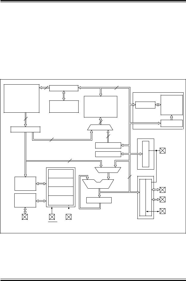
The PIC16F84A belongs to the mid-range family of the PICmicro™ microcontroller devices. A block diagram of the device is shown in Figure 1-1.
The program memory contains 1K words, which translates to 1024 instructions, since each 14-bit program memory word is the same width as each device instruction. The data memory (RAM) contains 68 bytes. Data EEPROM is 64 bytes.
There are also 13 I/O pins that are user-configured on a pin-to-pin basis. Some pins are multiplexed with other device functions. These functions include:
•External interrupt
•Change on PORTB interrupt
•Timer0 clock input
Table 1-1 details the pinout of the device with descriptions and details for each pin.
FIGURE 1-1: |
PIC16F84A BLOCK DIAGRAM |
|
|
|
|
|
|
||
|
13 |
Program Counter |
Data Bus |
8 |
|
|
|
||
Flash |
|
|
|
|
|
EEPROM Data Memory |
|||
|
|
|
|
|
|
|
|||
|
|
|
|
|
|
|
|
|
|
Program |
|
|
|
|
|
|
|
|
|
Memory |
|
|
|
RAM |
|
|
|
|
|
|
|
|
|
|
|
|
|
EEPROM |
|
PIC16F84A |
8 Level Stack |
File Registers |
|
|
EEDATA |
Data Memory |
|||
1K x 14 |
|
|
(13-bit) |
PIC16F84A |
|
|
|
64 x 8 |
|
|
|
|
|
|
|
|
|
||
|
|
|
|
68 x 8 |
|
|
|
|
|
Program |
14 |
|
|
|
|
|
|
|
|
Bus |
|
|
7 |
RAM Addr |
|
|
EEADR |
||
|
|
|
|
|
|||||
|
|
|
|
|
|
|
|
|
|
Instruction reg |
|
|
Addr Mux |
|
|
|
|
||
|
|
|
|
|
|
|
|
||
|
|
5 |
Direct Addr |
|
7 |
Indirect |
|
TMR0 |
|
|
|
|
|
Addr |
|
|
|
||
|
|
|
|
|
|
|
|
|
|
|
|
|
|
FSR reg |
|
|
|
||
|
|
|
|
STATUS reg |
|
|
RA4/T0CKI |
||
|
|
|
|
|
|
|
|||
|
|
|
8 |
|
|
|
|
|
|
|
|
Power-up |
|
MUX |
|
|
|
||
|
|
|
|
|
|
I/O Ports |
|
||
|
|
Timer |
|
|
|
8 |
|
||
|
|
|
|
|
|
|
|||
Instruction |
Oscillator |
|
|
|
|
|
|
||
Decode & |
Start-up Timer |
ALU |
|
|
|
|
|
||
Control |
|
|
|
|
|
|
|
||
Power-on |
|
|
|
|
|
|
|||
|
|
|
|
|
|
|
RA3:RA0 |
||
|
|
Reset |
|
|
|
|
|
|
|
Timing |
Watchdog |
W reg |
|
|
|
|
RB7:RB1 |
||
Generation |
Timer |
|
|
|
|
|
|
||
|
|
|
|
|
|
|
|
|
RB0/INT |
OSC2/CLKOUT |
MCLR |
VDD, VSS |
|
|
|
|
|
|
|
OSC1/CLKIN |
|
|
|
|
|
|
|
|
|
1998 Microchip Technology Inc. |
Preliminary |
DS35007A-page 3 |

PIC16F84A
TABLE 1-1 |
PIC16F84A PINOUT DESCRIPTION |
|
|
||||||
|
|
|
|
|
|
|
|
|
|
|
Pin Name |
DIP |
SOIC |
SSOP |
I/O/P |
Buffer |
|
Description |
|
|
No. |
No. |
No. |
Type |
Type |
|
|||
|
|
|
|
|
|||||
|
|
|
|
|
|
|
|
|
|
|
|
|
|
|
|
|
|
|
|
|
OSC1/CLKIN |
16 |
16 |
18 |
I |
ST/CMOS (3) |
|
Oscillator crystal input/external clock source input. |
|
|
OSC2/CLKOUT |
15 |
15 |
19 |
O |
— |
|
Oscillator crystal output. Connects to crystal or resonator in |
|
|
|
|
|
|
|
|
|
|
crystal oscillator mode. In RC mode, OSC2 pin outputs |
|
|
|
|
|
|
|
|
|
CLKOUT which has 1/4 the frequency of OSC1, and |
|
|
|
|
|
|
|
|
|
denotes the instruction cycle rate. |
|
|
|
|
|
|
|
|
|
|
|
|
|
4 |
4 |
4 |
I/P |
ST |
|
Master clear (reset) input/programming voltage input. This |
|
MCLR |
||||||||
|
|
|
|
|
|
|
|
|
pin is an active low reset to the device. |
|
|
|
|
|
|
|
|
|
|
|
|
|
|
|
|
|
|
|
PORTA is a bi-directional I/O port. |
|
RA0 |
17 |
17 |
19 |
I/O |
TTL |
|
|
|
|
RA1 |
18 |
18 |
20 |
I/O |
TTL |
|
|
|
|
RA2 |
1 |
1 |
1 |
I/O |
TTL |
|
|
|
|
RA3 |
2 |
2 |
2 |
I/O |
TTL |
|
|
|
|
RA4/T0CKI |
3 |
3 |
3 |
I/O |
ST |
|
Can also be selected to be the clock input to the TMR0 |
|
|
|
|
|
|
|
|
|
|
timer/counter. Output is open drain type. |
|
|
|
|
|
|
|
|
|
|
|
|
|
|
|
|
|
|
|
PORTB is a bi-directional I/O port. PORTB can be software |
|
|
|
|
|
|
|
|
|
programmed for internal weak pull-up on all inputs. |
|
RB0/INT |
6 |
6 |
7 |
I/O |
TTL/ST (1) |
|
RB0/INT can also be selected as an external interrupt |
|
|
|
pin. |
|||||||
|
|
|
|
|
|
|
|
|
|
|
RB1 |
7 |
7 |
8 |
I/O |
TTL |
|
|
|
|
RB2 |
8 |
8 |
9 |
I/O |
TTL |
|
|
|
|
RB3 |
9 |
9 |
10 |
I/O |
TTL |
|
|
|
|
RB4 |
10 |
10 |
11 |
I/O |
TTL |
|
Interrupt on change pin. |
|
|
RB5 |
11 |
11 |
12 |
I/O |
TTL |
|
Interrupt on change pin. |
|
|
RB6 |
12 |
12 |
13 |
I/O |
TTL/ST (2) |
|
Interrupt on change pin. Serial programming clock. |
|
|
RB7 |
13 |
13 |
14 |
I/O |
TTL/ST (2) |
|
Interrupt on change pin. Serial programming data. |
|
|
VSS |
5 |
5 |
5,6 |
P |
— |
|
Ground reference for logic and I/O pins. |
|
|
|
|
|
|
|
|
|
|
|
|
VDD |
14 |
14 |
15,16 |
P |
— |
|
Positive supply for logic and I/O pins. |
|
|
|
|
|
|
|
|
|
|
|
Legend: |
I= input |
O = output |
I/O = Input/Output |
P = power |
|
|
— = Not used |
TTL = TTL input |
ST = Schmitt Trigger input |
Note 1: |
This buffer is a Schmitt Trigger input when configured as the external interrupt. |
|||
2:This buffer is a Schmitt Trigger input when used in serial programming mode.
3:This buffer is a Schmitt Trigger input when configured in RC oscillator mode and a CMOS input otherwise.
DS35007A-page 4 |
Preliminary |
1998 Microchip Technology Inc. |