

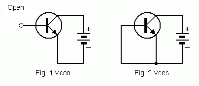
Vceo and Vces
What is the difference between the two? Which should actually be applied as the maximum voltage between the collector and emitter?
Taking
the rated voltage as an example for the voltage rating method, the
voltage is applied between the collector and emitter using the
emitter as the reference, and rated according to the base pin status.
In other words, Vceo (Fig. 1) is the rating between the collector
and emitter for base open, and Vces (Fig. 2) is the rating between
the collector and emitter when a short circuit is established between
the base and emitter.
Since the relationship between Vceo and
Vces is Vceo < Vces, safety is achieved by complying with the
lowest of the two, Vceo.
Vebo is a breakdown voltage or max voltage with the emitter-base junction reverse biased. In normal circuit operation, this junction is forward biased.
Vc is the voltage at the collector. To ensure you do not exceed the BVceo spec, you would want to measure or calculate the highest possible Vc that the circuit could see or generate, and then compare that to the datasheet value of BVceo.
To check Vb against Vebo, you see what the highest negative base voltage (for NPN) your circuit can see and compare that to the datasheet value of BVebo.
Vcbo is usually not an issue as it is significantly lower than the BVceo (spec).
To check Vb against BVebo, you see what the highest negative base voltage (for NPN) your circuit can see and compare that to the datasheet value of BVebo
Vcbo is usually not an issue as it is significantly lower than the BVceo (spec).
For a simple class A amplifier, the Vc max would be the collector supply voltage. It's only with inductive loads that the collector voltage can get above the supply voltage, and then it depends on the input voltages and the nature of the collector load impedance. Difficult to calculate, usually in these cases, a BVceo rating of twice the supply would be ok, but there are exceptions, such as a flyback amplifier, where the collector voltage is much higher than that. So it really depends on the circuit and the input drive.
For Vebo, which has a max rating of usually 5 to 7 volts, to cause problems, means you need a voltage applied to the base that has a negative peak exceeding that voltage. If you think this could happen, a diode will protect against that. Again, it really depends on the circuit and the input drive.
.
Task 2
Use Table 1 and these explanations of the column headings to answer the questions which follow.
|
Heading |
Explanation |
|
Case style |
transistor case and pin connections |
|
VCЕ0 (max) |
maximum value of collector-emitter voltage with base left open-circuit |
|
VCB0 (max) |
maximum value of collector-base voltage with emitter left open-circuit |
|
VEB0 (max) |
maximum value of (reverse) emitter-base voltage with collector left open-circuit |
|
Iс (max) |
maximum value of collector current |
|
PT0T (max) |
maximum total power dissipation |
|
Тур hFE |
typical small-signal current gain (in common-emitter configuration) |
|
@ Ic |
value of collector current at which the small-signal current gain is quoted |
|
Тур fT |
transition frequency (i.e. the frequency at which the common-emitter current gain falls to 1) |
|
Application |
recommended use for the device |
-
What's the recommended use for a BC214L?
-
What's the maximum collector current for a BC169C?
-
Which transistor can be used in a complementary configuration with a BC183L?
-
Could you use a BC109C in a circuit where the collector-emitter voltage will be in the range 10-30 volts?
-
What is the common-emitter current gain for a BC168C at a frequency of 85Mhz?
Task 3
Working with your partner, try these more difficult questions. You have the following transistors available: BC168C, BC169C, BC212L, BC214L. Which of them is most suitable for use in a circuit:
-
with a collector current greater than 100mA and a collector-emitter voltage between -10V and -35V?
-
with a common-emitter current gain greater than 100 and a collector current greater than 100mA?
-
which requires a common-emitter current gain greater than 200 at a frequency of 100MHz?
-
which is a low noise preamp with a collector current greater than 80mA?
-
with a collector current of 70mA and a common-emitter current gain greater than 600?
 Task
4
Task
4
Writing 1 Describing transistor characteristics
Complete this description of a BC108C using the information in Table 1 and the explanations in Task 2.
The BC108C is an NPN transistor with a _________________1 style case. It can pass a maximum collector current of ____________________2 mA.
With the base left open, the collector-emitter junction would break down at _______________3 V. The collector-base breakdown _________________4, with the emitter disconnected, is 30V. The ________________5 junction breakdown voltage is 5V when the collector is left open. These are the highest usable voltages for this transistor.
The transistor dissipates a_________________6 power of 300mW. When connected in common-emitter configuration, the small-signal current gain is 520 measured at a collector current of ________________7 mA. Typically, this gain would be reduced to 1 at a frequency of ____________________8 MHz. The transistor is a ___________________9 device which can be used in complementary configuration with a ________________10.
Task 5
Now write your own description of a BC214L, based on the text you have just completed in Task 4.
Technical reading Combinational logic
Task 1
Answer the following questions about the text below.
1. What terms are used in the text for each of the following?
-
a digital switching circuit.
-
the output of each gate depending on the combination of its inputs.
-
the number of ICs used in a computer.
-
an indication of the number of components used in an IС.
2. What is shown by:
-
a truth table?
-
a pin-out diagram?
3. What is another name for a NOT gate?
4. What are the two common families of logic ICs?
5. What do these abbreviations stand for?
-
TTL
-
VLSI
-
CMOS
-
MSI
6. Which of these statements are true for CMOS ICs?
-
They contain bipolar transistors.
-
They contain field effect transistors.
-
They are particularly suitable for use in battery-operated portable computers.
-
They are particularly suitable for use in large, high-speed computers
The decision-making circuits used in modern computers are mainly composed of combinations of digital switching circuits known as logic gates. Fig. 1 shows the logic symbols and truth tables for some basic gates.
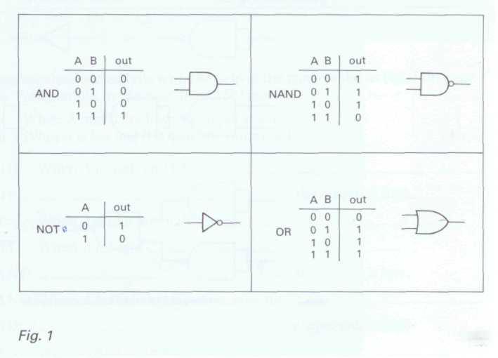
The output of each gate depends on the combination of its inputs. This is known as combinational logic. The output for all possible inputs is shown using a truth table. The truth tables show that the output of an AND gate is only high (i.e. logic level 1) when all its inputs are high. The output of a NAND gate, however, stays high unless all its inputs are high. The output of a NOT gate (also known as an inverter) is always the opposite of its input.
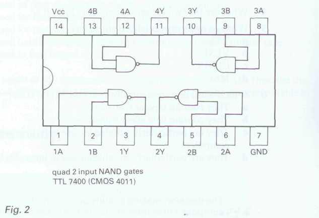
Computers use ICs which contain a number of logic gates on one chip. An IС pin-out diagram shows the arrangement of the gates and the function of each pin on the chip (see Fig. 2).
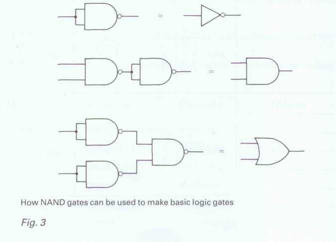
The number of ICs used in a computer, i.e. the chip count, can be reduced by connecting NAND gates together to form other types of gates (see Fig. 3).
The number of components in an IС is indicated by its scale of integration as shown in Table 1. The IС shown in Fig. 2 is an SSI device but microprocessors used in computers are VLSI or SLSI devices.
Table 1
|
Scale of integration |
Abbreviation |
No. of active components |
|
Small-scale integration |
SSI |
1 to 10 |
|
Medium-scale integration |
MSI |
10 to 102 |
|
Large-scale integration |
LSI |
102 to 103 |
|
Very large-scale integration |
VLSI |
103 to 104 |
|
Super large-scale integration |
SLSI |
104 to 105 |
There are two common families of logic ICs used in computers. TTL (transistor-transistor logic) ICs use bipolar transistors to form each gate whereas CMOS (complementary metal oxide semiconductor) ICs use field effect transistors (FETs). The different characteristics of each family determine which will be used in a particular computer (see Table 2). For example, TTL ICs are used in large, high-speed computers and CMOS ICs are better for battery-powered portable computers.
Table 2
|
Properties |
TTL |
CMOS |
|
Supply voltage |
+5V±0.25% |
+3V to+15V |
|
Supply current |
mA |
mА |
|
Power dissipation |
mW |
mW |
|
Switching speed |
fast |
relatively slow |
|
Input impedance |
low |
high |
Task 2
Complete these statements with the help of the truth tables in Fig. 1. For example, in the case of an AND gate:
-
When A and В are low, the output is low.
-
When A is low and В is high, the output is low.
|
1 |
AND |
When A is high and В is low, _____________________________. |
|
2 |
NOT |
_______________________________________, the output is high. |
|
3 |
OR |
When A and В are high, _________________________________. |
|
4 |
NOT |
When A is high, _______________________________________. |
|
5 |
NAND |
_______________________________________, the output is low. |
|
6 |
NAND |
When A is high and В is low, _____________________________. |
|
7 |
AND |
_______________________________________, the output is high. |
|
8 |
NAND |
When A and В are low, __________________________________. |
Task 3
Writing Explaining a process control system
Study this diagram. It shows how an industrial process is controlled using logic gates. With the help of the diagram, complete the blanks in the explanation which follows. Each blank may be one or more words.
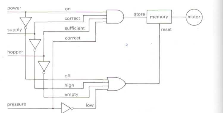
A motor controlling the flow of aluminium blanks to a hydraulic press is switched on only under these conditions:
-
The power is on.
-
The supply voltage is _____________________1.
-
There are ___________________2 aluminium blanks in the hopper (store).
-
The _________________3 in the hydraulic press is correct.
Information on these four conditions is fed into an ________________4 as all four conditions must be satisfied for the motor to run. When _______________5, the output from the AND gate is high. This is fed into the store input of the ______________6 unit to provide a continuous signal to operate the motor.
The motor must stop if any one of these conditions occurs:
-
The power is ________________7.
-
The ___________________8 rises.
-
The hopper is _______________9.
-
The _________________10 drops.
Information on each of these conditions is fed through a ________________11.When the input is low, ________________12.The output from each NOT gate is fed to an ______________13. When any of the four inputs to the OR gate is high, the output ______________14. When this is fed to the memory reset, it interrupts the continuous signal to the motor. The motor is switched _________________15 and the flow of aluminium blanks to the press is thus _______________________16.