

Single photon sources and detectors
.pdf071101-10 Eisaman et al. |
Rev. Sci. Instrum. 82, 071101 (2011) |
TABLE II. Comparison of single-photon detectors based on a table from Ref. 309 using a figure of merit given by the ratio of the detection efficiency to the product of the dark-count rate and the time resolution (assumed to be the timing jitter), η/(Dδt). Maximum count rate is a rough estimate from the the detector’s output pulse width or count rate that yields 100% dead time. The photon-number-resolving (PNR) capability is defined here as: none) for devices that are typically operated as a photon or no photon device, some) for devices that are made from multiple detectors that individually have no PNR capability and thus are limited in the photon number that can be resolved to the number of individual detectors, and full) for devices whose output is inherently proportional to the number of photons even if their proportional response ultimately saturates at high photon levels.
|
|
Detection |
Timing |
Dark-count |
|
Max. |
|
|
|
|
Operation |
efficiency, |
jitter, |
rate, D |
Figure |
count |
|
|
|
|
temperature |
wavelength |
δt(ns) |
(ungated) |
of |
rate |
PNR |
|
|
Detector type |
(K) |
η(%), λ (nm) |
(FWHM) |
(1/s) |
merit |
(106/s) |
capability |
Refs. |
|
|
|
|
|
|
|
|
|
|
|
PMT (visible–near-infrared) |
300 |
40 @ 500 |
0.3 |
100 |
1.3 × 10⁷ |
10 |
Some |
271, 272 |
|
PMT (infrared) |
200 |
2 @ 1550 |
0.3 |
200 000 |
3.3 × 10² |
10 |
Some |
273 |
|
Si SPAD (thick junction) |
250 |
65 @ 650 |
0.4 |
25 |
6.5 × 10⁷ |
10 |
None |
274 |
|
Si SPAD (shallow junction) |
250 |
49 @ 550 |
0.035 |
25 |
5.6 × 10⁸ |
10 |
None |
275 |
|
Si SPAD (self-differencing) |
250 |
74 @ 600 |
... |
2000 |
... |
16 |
Some |
276 |
|
Si SPAD (linear mode) |
78 |
56 @ 450 |
... |
0.0008 |
... |
0.01 |
Fulla |
277 |
|
Si SPAD (cavity) |
78 |
42 @ 780 |
0.035 |
3500 |
3.4 × 10⁶ |
10 |
None |
278 |
|
Si SPAD (multipixel) |
290 |
40 @ 532 |
0.3 |
25 000–500 000 |
1 × 10⁴ |
30 |
Some |
279, 280 |
|
Hybrid PMT (PMT + APD) |
270 |
30 |
@ 1064 |
0.2 |
30 000 |
5 × 10⁴ |
200 |
None |
281, 282 |
Time multiplexed (Si SPAD) |
250 |
39 @ 680 |
0.4 |
200 |
5 × 10⁶ |
0.5 |
Some |
234 |
|
Time multiplexed (Si SPAD) |
250 |
50 @ 825 |
0.5 |
150 |
7 × 10⁶ |
2 |
Some |
283 |
|
Space multiplexed (InGaAs SPAD) |
250 |
33 |
@ 1060 |
0.133 |
160 000 000 |
1.6 × 101 |
10 |
Some |
284 |
Space multiplexed (InGaAs SPAD) |
250 |
2 @ 1550 |
... |
... |
... |
0.3 |
None |
285 |
|
InGaAs SPAD (gated) |
200 |
10 |
@ 1550 |
0.370 |
91 |
3.0 × 10⁵ |
0.01 |
None |
286 |
InGaAs SPAD (self-differencing) |
240 |
10 |
@ 1550 |
0.055 |
16 000 |
1.1 × 10⁵ |
100 |
None |
287 |
InGaAs SPAD (self-differencing) |
240 |
10 |
@ 1550 |
... |
... |
... |
... |
Full |
267 |
InGaAs SPAD (discharge pulse counting) |
243 |
7 @ 1550 |
... |
40 000 |
... |
10 |
None |
288 |
|
InP NFAD (monolithic negative feedback) |
243 |
6 @ 1550 |
0.4 |
28 000 |
5 × 10³ |
10 |
Some |
289, 290 |
|
InGaAs (self-quenching and self-recovery) |
300 |
... @ 1550 |
10 |
... |
– |
3 |
Some |
291 |
|
CIPD (InGaAs) |
4.2 |
80 |
@ 1310 |
... |
... |
... |
0.001 |
Full |
263 |
Frequency up-conversion |
300 |
8.8 @ 1550 |
0.4 |
13000 |
1.7 × 10⁴ |
10 |
None |
292 |
|
Frequency up-conversion |
300 |
56-59@ 1550 |
... |
460000 |
... |
5 |
None |
254, 293 |
|
Frequency up-conversion |
300 |
20 |
@ 1306 |
0.62 |
2200 |
1.5 × 10⁵ |
10 |
None |
294 |
VLPC |
7 |
88 @ 694 |
40 |
20000 |
1.1 × 10³ |
10 |
Some |
295 |
|
VLPC |
7 |
40 @ 633 |
0.24 |
25000 |
6.7 × 10⁴ |
10 |
Some |
296 |
|
SSPM |
6 |
76 @ 702 |
3.5 |
7000 |
3 × 10⁴ |
30 |
Full |
297 |
|
TES(W) |
0.1 |
50 |
@ 1550 |
100 |
3 |
1.7 × 10⁶ |
0.1 |
Full |
298 |
TES(W) |
0.1 |
95 |
@ 1556 |
100 |
... |
... |
0.1 |
Full |
299 |
TES(Ha) |
0.1 |
85 @ 850 |
100 |
... |
... |
0.1 |
Full |
300 |
|
TES (Ti) |
0.1 |
81–98 @ 850 |
100 |
... |
... |
1 |
Full |
301–303 |
|
SNSPD |
3 |
0.7 @ 1550 |
0.06 |
10 |
1.2 × 10⁷ |
100 |
None |
304 |
|
SNSPD (in cavity) |
1.5 |
57 |
@ 1550 |
0.03 |
... |
... |
1000 |
None |
253 |
Parallel SNSPD |
2 |
2 @ 1300 |
0.05 |
0.15 |
2.7 × 10⁹ |
1000 |
Some |
262 |
|
STJ |
0.4 |
45 @ 350 |
2000 |
... |
... |
0.01 |
Full |
258, 259, 305 |
|
QD (resonant tunnel diode) |
4 |
12 @ 550 |
150 |
0.002 |
4 × 10⁹ |
0.25 |
Full |
306 |
|
QDOGFET (field-effect transistor) |
4 |
2 |
@ 805 |
10000 |
150 |
10 |
0.05 |
Full |
265, 307, 308 |
aPNR should be possible, but none has been demonstrated as of yet.
electronics. All this requires operation in vacuum. While we have put the PMT in the section with non-photon-number- resolving detectors, some models have low enough gain noise to make it possible to partially resolve output pulses resulting from different numbers of incoming photons, with the first such demonstration made by incorporating a first dynode specially prepared to yield higher electron emission.310, 311 We also note that a PMT can be used as an n-photon detector for wavelengths with energies below the bandgap so that more than one photon is needed to generate a photoelectron, albeit with greatly reduced detection efficiency and requiring tightly focused beams to enhance the multi-photon absorption process.312
The efficiency of PMTs is typically in the range of 10% to 40%, limited by the efficiency with which the incoming photon knocks out the initial photoelectron from the photosensitive surface (the photocathode). While these efficiencies are impressive for a pioneering technology, they fall short of the requirements of many modern applications. Other features of PMTs are the large sensitive areas (cm2 or even up to m2), fast response (low timing jitter and low dead time) with the capability to resolve photons separated by a nanosecond, and the low level of dark counts (output pulses that result from causes other than incident photons). The dark-count rates can be as low as a few events per second, particularly if the PMT is cooled by a few tens of degrees C. Their major drawbacks
Downloaded 01 Oct 2011 to 87.117.190.67. Redistribution subject to AIP license or copyright; see http://rsi.aip.org/about/rights_and_permissions
071101-11 Eisaman et al.
Photocathode Photon
Electrical connections
Anode
Electron
Dynode
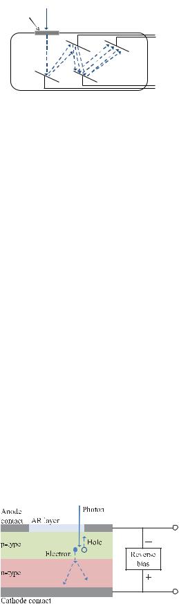
FIG. 6. (Color online) A photomultiplier, the first detector able to sense a single optical photon, is shown schematically with a transmissive photocathode and just 3 dynodes. The photocathode may be designed to have the photoelectrons emitted from its front or back surface and typically 10 dynodes are used.
include their reliance on vacuum tube technology which limits their lifetime, reliability, and scalability.
2. Single-photon avalanche photodiode
The SPAD (Fig. 7) uses a similar process to the PMT, but the initial photon absorption creates an electron-hole pair and the charge multiplication is continuous, with a voltage applied across a semiconductor lattice rather than between discrete dynodes suspended in vacuum. SPADs are typically run in what is referred to as “Geiger-mode,” where a bias voltage greater than the diode’s breakdown voltage is applied. Thus when a charge is generated by an incoming photon, the charge multiplication (or avalanche) proceeds until it saturates at a current typically limited by an external circuit, and that current is self-sustaining. The saturated avalanche current must be terminated by lowering the bias voltage below the breakdown voltage before the SPAD can respond to a subsequent incoming optical pulse. This saturation means that gain in Geiger mode is not a useful concept. Geiger-mode SPADs can have detection efficiencies higher than PMTs, up to 85% (for Si SPADs in the visible), although SPAD dark-count rates and timing jitter are somewhat higher than the best PMTs and for IR SPADs, efficiencies are in the 10% to 20% range with darkcount rates much higher than PMTs.247, 250 To reduce darkcount rates, SPADs are typically cooled with thermoelectric coolers to temperatures of 210 K to 250 K.
In addition, the SPAD gain medium typically has trap sites that must be allowed time to depopulate after an
FIG. 7. (Color) A single-photon avalanche photodiode is shown with distinct regions for the photo-absorption and carrier multiplication processes. The voltage is applied to accelerate the electrons toward the multiplication region. A front-illuminated geometry with an antireflection (AR) coating to improve efficiency is illustrated, but back-illuminated designs are also used.
Rev. Sci. Instrum. 82, 071101 (2011)
avalanche has occurred and before the bias voltage can be restored. If those sites are not allowed to depopulate, a second avalanche can be initiated by carriers released from traps rather than from a new photon. This “afterpulsing” effect necessitates additional waiting time after a pulse before rebiasing the device. As a result, SPAD dead times can range from tens of nanoseconds to 10 μs. This is a particular problem for SPADs designed for IR sensitivity.
There are a number of schemes focused on these issues to reduce dead time or its effect,285 to reduce afterpulsing (e.g., by detection multiplexing to maximize the time recovery between firings of a single detector285 and by self-differencing of adjacent pulses to reduce avalanche currents and output transients relative to the avalanche signal of interest249), to improve IR performance, and to realize some photon- number-resolution capability. Efforts toward photon-number- resolution are discussed in Sec. III C. Some design techniques can result in very low time-jitter detectors. These usually involve thinner absorption regions so there can be a tradeoff between detection efficiency and timing jitter, although there is an effort to regain some efficiency by using cavity enhancement around the thinner absorber.278 An in-depth look at the details of this type of tradeoff can be found in Ref. 313 and a commercial example of this tradeoff can be seen in Ref. 275.
While all commercial SPADs operate in Geiger-mode, there are efforts to develop linear-mode operation for photon counting. This would have the advantages of having an output that is proportional to the number of incident photons, yielding photon-number resolution, lower afterpulsing due to lower current flow and less trap filling, and reduced dead time. The smaller current pulses generated in the linear mode require long measurement times to reduce the readout noise and thus in one recent demonstration a 56% detection efficiency and 0.0008 /s dark-count rate was achieved, but at a 10 kHz maximum repetition rate.277 While these linear devices can in principle provide photon-number resolution, the noise on the gain and the smaller signals involved can broaden the output current pulse amplitudes so much that pulses due to different numbers of incident photons cannot be resolved. We are unaware of any demonstrated number resolution of these devices.
Having just described PMT and SPAD detectors, we note that there is a detector that is essentially a hybrid between the two. It consists of a photocathode and electron impact multiplication stage in vacuum providing gain ≈103 followed by an avalanche diode multiplication region for a total gain above 104. This arrangement allows for a photocathode optimized for a particularly difficult wavelength for photon counting detectors, 1060 nm, with efficiency of 30% and a low dark-count rate of 30 000 counts/s.281, 282
3. Quantum-dot field-effect transistor-based detector
A quantum dot in conjunction with a field-effect transistor (FET) has been reported to offer single-photon sensitivity in the near IR. This detector design, sometimes referred to as a QDOGFET,265, 307, 308 consists of an optical absorber with a thin layer of quantum dots between
Downloaded 01 Oct 2011 to 87.117.190.67. Redistribution subject to AIP license or copyright; see http://rsi.aip.org/about/rights_and_permissions
071101-12 Eisaman et al.
the gate electrode and conduction channel in an FET. The photo-generated charges move to the quantum dots where they are trapped. Those trapped charges shield the gate potential and thus modify the channel conductance of the FET. In one implementation, the trapped carriers are holes that reduce the negative field of the quantum dots allowing the conductivity to increase.175 Thus current can flow unimpeded until the photon-generated carrier is removed or recombines, yielding an observable single-photon signal. We also note a detector that operates on the same scheme as the QDOGFET but instead uses native traps, rather than quantum dots, to store the photo-generated charges.314
Another quantum dot-based approach uses the photogenerated carriers to enhance resonant tunneling through a double barrier. By adjusting the field so that the well between the two barriers matches the energy of the band on the other side of one of the barriers, the tunneling rate increases dramatically and in proportion to the number of incident photons. In this scheme the photo-generated holes trapped by the quantum dots provide the field necessary to shift that intermediate band into resonance.306 We note a detector that works on a similar principle but because it operates in the far IR it is beyond the scope of this review.252
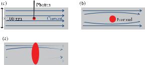
4. Superconducting nanowire single-photon detector
This fast (timing jitter <50 ps) single-photon detector relies on a narrow superconducting wire that is biased with a current at a level just below the critical current density, above which the wire must revert to normal resistance253, 315–317 (Fig. 8). In this state, when an incoming photon is absorbed, its energy causes a small spot of the wire to go normal. This in turn causes the current to flow around the normal resistance region and as a result the current density is increased in those adjacent regions. Those adjacent regions now exceed the critical current density and a normal resistance region is formed all the way across the width of the wire. This small normal region of the superconducting wire yields a voltage spike that indicates the detection of a single photon. Because this detection mechanism requires a very narrow wire (≈100 nm), a meandering surface-filling arrangement of the wire is used to create a practical sensitive area. In addition, devices fabricated with a mirror on top of the nanowire meander made of NbN, thus forming an optical cavity have achieved detection efficiencies in the neighborhood of 25%.318, 319 In these devices the light first passes through the NbN substrate subject to reflective losses. Subsequent devices have achieved efficiencies (not including light missing the detector active area) of 57% and 67% at 1550 nm and 1064 nm respectively,253 by adding an antireflection coating to the input side of the cavity device. These detectors do not suffer afterpulsing, although they can latch320 into a mode where they stay in the normal state due to self-heating of the normal region and have to be actively reset by reducing the current flow. Because these detectors require superconductivity, their operating temperatures are typically in the range of 4 K or less.
While the arrangement just described cannot discriminate between one or more incident photons, as we shall see in
Rev. Sci. Instrum. 82, 071101 (2011)
FIG. 8. (Color online) A section of a superconducting nanowire singlephoton detector is shown with a bias current just below the critical current density that would drive the wire normal. (a) An incoming photon creates a small normal region within the nanowire. (b) The superconducting current is expelled from the normal region, increasing the current density in the adjacent areas of the nanowire. (c) That increase in current density is enough to drive those adjacent regions normal, which in turn results in a measurable voltage drop across the detector.
Sec. III C 3 there are efforts to provide this detector with some photon-number-resolving capability.262, 319
5. Up-conversion single-photon detector
Up-conversion of a photon from the infrared, where detector characteristics are typically poor, to the visible spectral region, where detector performance is better, has been demonstrated by a number of research groups321 and has been commercialized.272, 322 The scheme uses sum-frequency generation in a nonlinear crystal, where a strong pump beam mixes with the IR single photon of interest to create a single photon at the sum frequency in the visible. Both visible SPADs and PMTs have been used for the detection of the upconverted photon. The key drivers for these efforts are better detection efficiency at low dark-count rates, and higher count rates with better pulse-pair resolution. The overall efficiency of this approach is the product of the optical conversion efficiency, the optical losses throughout the system, and the visible detector efficiency. The up-conversion step has been demonstrated with near unit efficiency,293 with the other factors limiting the overall efficiency to 56% to 59% to date.254, 293, 321, 323 Background count rates are also of concern as the up-conversion process can produce a significant number of unwanted photons. To address this, having the upconversion pump photon at an energy lower than the IR photon to be up-converted rather than the other way around, may prove advantageous in some applications.294 This avoids having the pump beam create Raman photons at the wavelength of interest that are then up-converted as if they were incident IR photons.
C. Photon-number-resolving detectors
Developing photon-number-resolving (PNR) detectors is important for many applications in quantum-information science, such as quantum computation using linear optics324 and quantum communication.15 Section IV describes how photon-number resolution impacts quantum communication protocols.
Downloaded 01 Oct 2011 to 87.117.190.67. Redistribution subject to AIP license or copyright; see http://rsi.aip.org/about/rights_and_permissions
071101-13 Eisaman et al.
One direct approach to gaining photon-number-resolving capability is to simply break the detector active area into many distinct areas or pixels, so that each can register a photon independent of the others; and when they do, only the pixel or pixels that detected a photon suffers a dead time and recovery time. Thus we have a multiple-pixel device where each pixel cannot resolve photon number, but taken together they can resolve as many photons as there are separate pixels (if those photons happen to hit different pixels). For small numbers of pixels, requiring the photons to hit different pixels can be an issue, but as the number of pixels increase, the probability of hitting the same pixel with another photon decreases, resulting in a much more faithful approximation to true photon- number-resolving capability.
Before describing specific PNR detectors we should clarify what is meant by “photon-number-resolution.” It is important to lay out the degrees of photon-number-resolution that a detector can have. First we note that as mentioned earlier, photon-number-resolving does not mean that one determines the number of photons incident on the the detector. Without 100% detection efficiency, the measured number is at best just a lower estimate, and with dark counts it is not even that. This is particularly an issue for detectors with very low efficiency. In addition we attempt to categorize the degree of PNR capability into three groups defined as (a) “no PNR capability” for devices that are typically operated as a photon or no-photon device, (b) “some PNR capability” for devices made of multiple detectors that individually have no PNR capability and thus are limited in the maximum photon number that can be resolved to the number of individual detectors, and (c) “full PNR capability” for devices whose output is inherently proportional to the number of photons, even if their detection efficiency is low and their proportional response ultimately saturates at high input photons levels. (We are assuming relatively narrow band light incident on these detectors so that a detector with an output proportional to the incident energy is used to provide information on photon number, rather than the energy of those photons.) While this categorization is somewhat arbitrary, it is of some use in understanding the types of mechanisms used to produce PNR capability.
1. Superconducting tunnel junction (STJ)-based detector
One of the first superconducting photon-number- resolving detectors was the superconducting tunnel junction detector.258, 259, 305 In it photons are absorbed in a thin superconducting layer. The absorbed energy results in many broken Cooper pairs (quasiparticles) because the photon energy is ≈1000 times the energy needed to break Cooper pairs. That superconducting layer is separated from a second superconducting layer by an insulator that is thin enough (≈1 nm) to allow significant tunneling of the quasiparticles. A small bias voltage across this “superconducting tunnel junction” results in a current flow that is proportional to the photo-generated quasiparticles. A small magnetic field parallel to the barrier, along with a bias voltage that is low enough, prevents unbroken Cooper pairs from tunneling across the junction. As the device is operated significantly (≈10 times) below the super-
Rev. Sci. Instrum. 82, 071101 (2011)
conducting critical temperature, there are many fewer thermally generated quasiparticles than photo-generated quasiparticles, so single-photon detection is possible.
Because the current produced by this device is proportional to the incoming photon energy, it can resolve photon number. It has been demonstrated for wavelengths between 200 nm to 500 nm, limited on the long wavelength end by its energy resolution (≈100 nm at a wavelength of 300 nm). Devices have been demonstrated with detection efficiencies of >45% as estimated by reflectance and transmittance calculations at counts rates of ≈10 kHz at an operating temperature of 0.37 K.305 Background count rates are very low (<0.1% of photo-generated counts) and mostly limited by electronic noise, although thermal blackbody photons may also contribute.
2. Quantum-dot field-effect transistor-based detector
The QDOGFET detector, as discussed earlier, uses photo-generated charges to modulate electrical conductance and that modulation is proportional to those charges, thus this device has PNR capability and has been demonstrated with a detection efficiency of ≈2% at 805 nm.265, 307, 308 This implementation was shown to distinguish 0, 1, 2, and greater than 3 photons, with the percent of correct assignments for these four bins being 94%, 89%, 83%, and 90%, respectively. As shown in Table II, the QDOGFET has a low detection efficiency (2%) with a repetition rate of 50 kHz and a very low dark-count probability of 0.003/gate.
The quantum dot detector based on modulation of a resonant tunneling through a barrier also has been demonstrated to have a range of few photons of PNR capability with detection efficiency of ≈12% at 550 nm with and a dark count rate of 2000/s (Ref. 175) (Another implementation of this scheme showed linear operation which indicates the potential for PNR operation306). The dark count rate can be improved by an order of magnitude at a cost of reducing the detection efficiency to 5%. The operating temperature of this detector is 77 K, although faster operation was obtained at 4 K.
3. Superconducting nanowire-based single-photon detector
In Sec. III B 4, we discussed the principle behind superconducting-nanowire single-photon detectors. Two schemes have recently built upon that principle to demonstrate devices with some photon-number-resolving capability. Both achieve this by using several distinct nanowires to fill the active area rather than just a single nanowire.
The first of these schemes, the parallel-SNSPD,262 uses nanowires connected electrically in parallel. The currents through the parallel wires are summed so that the single analog output signal is proportional to the number of wires that have gone normal due to incident photons. This arrangement offers the potential of even faster operation speed than the already fast single SNSPD, because the inductance of the individual wires is much lower than the longer single-wire meander of the original SNSPD, whose temporal response is
Downloaded 01 Oct 2011 to 87.117.190.67. Redistribution subject to AIP license or copyright; see http://rsi.aip.org/about/rights_and_permissions
071101-14 Eisaman et al.
inductance limited.325 This scheme was demonstrated with niobium nitride (NbN) nanowires 100 nm wide with a capability of counting up to four photons, a dark-count rate of 0.15 Hz, and a repetition rate of 80 MHz. While the parallelSNSPD performs well relative to other photon-number- resolving detectors in regards to dark-count rate and repetition rate, as shown in Table II, most other detectors outperform the parallel-SNSPD detection efficiency of 2% at 1300 nm.262
The second scheme also runs parallel wires, but does so as completely separate detectors with individual outputs, thus the result is a digital output i.e., the number of output pulses gives the number of photons detected. This scheme was demonstrated in a system of four separate wires with a reported system detection efficiency of 25%.319
4. Superconducting transition edge sensor
The superconducting transition edge sensor operates as a bolometer, that is electromagnetic radiation is absorbed, and then that absorbed energy is detected as a rise in temperature. To achieve the extreme sensitivity required to detect the energy of a single photon, the heat capacity of the absorber must be made extremely small and the thermal sensor must exhibit a large response to a small temperature change. As a thermal device which measures energy absorbed, its output is proportional to the number of photons absorbed, thus it can provide photon-number resolution.
The extreme temperature sensitivity is achieved by constructing the thermal sensor from a thin layer of superconducting material (deposited on an insulating substrate) made to operate at a temperature in its transition between superconducting and normal resistance, so a slight change in temperature yields a large change in resistance. The device is maintained at this temperature through negative electro-thermal feedback. This works by applying a constant voltage bias across the film which increases the temperature of the electrons in the sensor film above the temperature of the substrate. When a photon is absorbed, the temperature of the sensor rises, which increases its resistance, which in turn reduces the current flowing through the sensor and thus reduces the Joule heating of the device. Thus the constant voltage bias and this electro-thermal feedback work to maintain the sensor at a set temperature within its superconducting transition temperature region, and the signal due to a photon is seen in a reduction in the current flowing through the sensor. Further sensitivity is achieved by measuring that current change using a superconducting quantum-interference device (SQUID) array.
The heat capacity of the sensor is reduced by fiber coupling the light to the device. By placing the fiber end just a few tens of μm from the sensor, the sensor can be made small, typically 25 μm across. In addition, operating at the low temperatures required for the superconducting transition operation further lowers the heat capacity. Note that the relevant heat capacity is that of the electrons in the superconductor and it is important that the thermal link between these electrons and the phonons in the substrate is low, which is the case at the temperatures of these devices, typically ≈100 mK. This weak thermal coupling of the electrons to phonons provides a link
Rev. Sci. Instrum. 82, 071101 (2011)
to a thermal heat sink that allows the electrons to slowly cool after quickly heating up upon photon absorption.
Since single-photon sensitivity was first demonstrated in the visible and IR,326 TES devices of high efficiency have been demonstrated with superconductors made of tungsten,299 titanium,301, 303, 327 and hafnium,300 and because they rely on simple absorption of the incident radiation followed by conversion to heat, their wavelength sensitivity can be tailored by appropriate antireflection coatings on the sensor surface. And most recently these devices have been fabricated using a design that self-aligns the fiber to the sensor area, facilitating reliable and robust high-efficiency assembly and construction, important steps toward a scalable detector.328
From Table II, we also see that the highest detection efficiency among PNR detectors is achieved by the transitionedge sensor (TES) detectors,299 with a detection efficiency of 95% for an incident wavelength of 1556 nm and 81% to 98% at 850 nm.300–302 We also note that these detectors provide some of the best visibility between photon-number-resolved peaks of any visible detector.257 Despite these high detection efficiencies and very low dark-count rates, drawbacks generally include a slow response of ≈100 ns and low maximum counting rates of ≈100 kHz (although Ref. 301 reports maximum count rates up to 1 MHz), and the need to operate at temperatures less than 100 mK.257
5. Visible light photon counter
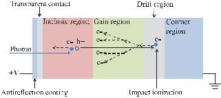
As seen in Table II, another detector that achieves quantum efficiencies almost as high as the TES is the visible light photon counter,113, 264 with a detection efficiency of up to 88% at 694 nm.295 A photon incident onto a VLPC detector will first encounter an intrinsic silicon layer followed by a gain layer that is lightly doped with arsenic (see Fig. 9, and Fig. 1 of Ref. 264). An incident photon can be absorbed either in the intrinsic silicon layer or the doped gain layer, creating an electron-hole pair. A bias voltage of 6 V to 7.5 V accelerates the electron (hole) away from (toward) the gain region. The gain region containing the As impurities lies 54 meV below the conduction band. Holes that are accelerated in the gain region impact ionize these impurities,
FIG. 9. (Color) Principle of operation of a visible light photon counter (VLPC). A single photon absorbed in the intrinsic region creates an electronhole pair. The applied voltage accelerates the electron towards the transparent contact on the left, and accelerates the hole to the right. The gain region is doped with As impurities. Holes accelerated into the gain region impact-ionize these impurities, exciting donor electrons into the conduction band. These electrons are accelerated towards the transparent contact and create additional impact ionization events, resulting in avalanche multiplication (Ref. 264).
Downloaded 01 Oct 2011 to 87.117.190.67. Redistribution subject to AIP license or copyright; see http://rsi.aip.org/about/rights_and_permissions
071101-15 Eisaman et al.
exciting donor electrons into the conduction band. These scattered electrons create further impact ionization events, resulting in avalanche multiplication. Assuming a single-photon absorption event always creates an electrical signal of the same magnitude, then the output electrical signal should simply be proportional to the number of detected photons. In practice, however, detectors that rely on multiplication gain have excess noise referred to as gain noise due to the fact that singlephoton absorption does not always produce an electrical signal of the same size. If the multiplication noise is too large (as it is for SPADs, for example), then photon-number resolution is very difficult or impossible. The VLPC, however, demonstrates nearly noise-free multiplication. The first reason is that due to the partial overlap of energy states of adjacent As impurities, holes left behind in the impurity state after impact ionization travel very slowly via conduction hopping, preventing the holes from producing further impact ionization events. Single-carrier multiplication (in this case, only the electrons are multiplied) has been shown to result in lower multiplication noise.264 The second reason for the low multiplication noise is that low electric fields are required because the As impurities are only 54 meV below the conduction band. This results in little variation in the time between ionization events, which has also been shown to reduce multiplication noise. This low multiplication noise is what allows for demonstrated photon-number resolving capability of the VLPC of photon numbers up to six (the probability of error in making the decision increases from 0.01% for zero photons to 11.3% for six photons).
The number resolution of the VLPC is due to the fact that the charge multiplication resulting from an incident photon is localized to spot a few microns across, so only that region suffers a dead time. The rest of the detector (typically 1 mm in diameter) remains ready to register additional photons with the output signal being the sum of those output pulses. With this localized dead region being such a small fraction of the total detector area, the number-resolved operation can be nearly complete, but one must be aware of this mechanism and avoid focusing the light too tightly on the detector or number resolution will be limited.264
While the efficiency and photon-number-resolution of the VLPC are impressive, the repetition rate (100 kHz) is low and the dark-count rate (20 kHz) is high.264 Very similar in design to the VLPC is the Solid-State Photomultiplier (SSPM),297 which has very broad spectral sensitivity ranging from 400 nm to 28 μm. The width of this range, while quite remarkable, has the drawback that it requires additional effort to shield the detector from any of the long-wave IR photons that might be out of the wavelength band of interest. In addition the availability of these detectors is very limited.
6. Other photon-number-resolving detectors
Other approaches to PNR detectors that we do not have the space to discuss in detail include the SPAD array284 (simply achieving photon-number resolution by having the optical mode impinge upon an array of parallel SPADs) that are read out individually284 or summed to give a single output
Rev. Sci. Instrum. 82, 071101 (2011)
pulse with amplitude proportional to photon number,279, 280 the time-multiplexed SPAD (Refs. 234, 283, 329) (This uses essentially the same idea as the spatial SPAD array, but splits up the mode into many temporal modes rather than many spatial modes. A detailed performance analysis can be found in Ref. 266.), and the charge integration photon detector (CIPD) (Ref. 263) (an InGaAs PIN photodiode connected to the gate of a GaAs junction gate field-effect transistor). The performance of these approaches relative to other PNR detectors can been seen in Table II.
One recent approach uses a single SPAD as a photonnumber resolving detector by measuring the slope of the avalanche rise (before saturation) to discern information about the number of incident photons.267, 276 This is done in conjunction with a self-differencing circuit that greatly reduces the size of the capacitive transient of the APD, which allows lower overbias voltages and lower thresholds to be used. It is reported that the combination of these advantages provides photon-number resolution for up to four photons at a wavelength of 1550 nm, detection efficiency of 10%, repetition rate of 622 MHz, and a dark-count rate of less than 2 × 10⁻⁶ per gate.267
D. Unique approaches to single-photon detectors
Other approaches to single-photon detection that are less well-known than the approaches discussed in Secs. III A–III C include QVDs,268 a proposal for a high efficiency PNR detector using an atomic vapor absorber, and a proposal for a quantum nondemolition (QND) single-photon-number-resolving detector that uses giant Kerr nonlinearities.270
QVDs are based on heat (Q)-to-voltage (V) conversion and digital (D) readout and rely on the thermoelectric effect that occurs when a junction between dissimilar materials is heated. Although theoretical analysis claims that such detectors offer the potential to count at rates of 100 MHz, photon counting in the visible using this method has yet to be demonstrated.268
It has been proposed that an atomic vapor with a threelevel -system plus an additional level can be used as the basis of a high efficiency PNR detector.269, 330 The scheme relies on the three-level -system plus an escort pulse to allow an incoming photon to transfer one atom to a metastable level where a second laser can cycle the atom many times in a closed two-level system, with the scattered photons being the indicator that a photon has been absorbed. The reliance on an atomic vapor absorber offers the potential for high absorption efficiency, and the cycling transition allows for many scattered photons for each atom transferred, which means high detection efficiency can be achieved. And because there would be a direct correspondence between the number of incident photons absorbed and the number of atoms undergoing the closed cycling transition, this scheme would be photon-number resolving.
A quantum nondemolition (QND) measurement is one where the state is determined, but is not destroyed in the measurement so that the now-known state remains available for other uses. Such a measurement for a photon-number state was proposed by Imoto et al.331 and discussed later in
Downloaded 01 Oct 2011 to 87.117.190.67. Redistribution subject to AIP license or copyright; see http://rsi.aip.org/about/rights_and_permissions
071101-16 Eisaman et al.
detail by others.270, 332, 333 The principle is to co-propagate the weak signal light pulse, whose number of photons is yet to be determined, with an stronger light pulse in a highly nonlinear medium. The intensity of the signal pulse changes the refractive index of the medium, which can then be seen as a phase change in the stronger copropagating light pulse. The key difficulty is that for the unknown few-photon state to produce a resolvable phase change in the copropagating pulse, the medium must have a very large optical nonlinearity. The photonic interactions such as Kerr-nonlinearity or cross-phase modulation for most media typically do not have large enough nonlinear coefficients. While generally far from implementation because of this difficulty, possible candidate media for the QND detection can be optical fiber, a high-quality factor cavity,334, 335 and electromagnetically induced transparency (EIT) in an atomic ensemble.270, 333 Recently Pryde et al.336 reported a QND measurement on the polarization state of single photons. It was pointed out and clarified that such a measurement on the polarization state is distinct from a QND measurement of photon number.337, 338
E. Electronics for single-photon detectors
As we have seen, single-photon detectors use a range of physical effects to detect a photon, however there is an important trend: most detectors work close to a critical regime so that a single photon changes the regime of operation. In the case of avalanche photodiodes, the p-n junction is reverse biased with a voltage that is somewhat higher than the breakdown voltage, so any single free carrier inside that p-n junction can start an avalanche. In a superconducting nanowire detector, the wire is biased with current just below the level that would drive the wire normal. The electronics in these devices is used to set correct bias voltages or currents, to monitor sudden changes of detector properties due to photoelectronic detection, and to return the device to its normal regime. In what follows, we discuss electronics design efforts specific to avalanche photodiodes, as that has been an area of significant effort and detection improvements.
A Geiger-mode avalanche photodiode operates reverse biased at a voltage V that is above the breakdown voltage Vb. A single free carrier (generated via a photoelectronic process) injected into the depletion layer triggers a self-sustaining avalanche. The current rise time is usually less than 1 ns. This current continues to flow until the bias voltage V is dropped. This process, referred to as quenching, is a main cause of dead time, because the detector cannot respond to incoming photons until the quenching is completed and the bias voltage is restored. Once the bias voltage is restored, the device is then ready to detect another photon. The operation just described requires a special circuit that does the following:
–detects the leading edge of the current pulse that corresponds to an avalanche,
–generates an output pulse exhibiting minimal jitter with respect to the avalanche pulse,
–lowers the bias to quench the avalanche, and
–restores the photodiode voltage to the operating level
V > Vb.
Rev. Sci. Instrum. 82, 071101 (2011)
If a detector is gated, then the circuit must apply reverse bias to the detector in synchronization with the incoming optical pulses and discriminate between pulses due to bias voltage transients and actual avalanche current, in addition to the above operations.
Given the numerous tasks required of the detector electronics, the features of the circuit dramatically affect the operating conditions of the detector and, as a consequence, the detector’s overall performance. The quenching mechanisms can be of three types: passive quenching, or active quenching circuits, or a combination of the two.
In passive systems, the avalanche current quenches itself. This approach is implemented with a very simple circuit - the photodiode is biased through a resistor that is small compared with the diode’s resistance when no avalanche is present and large compared with the diode’s residual resistance during avalanche process, typically 1 M to 100 k . When an avalanche occurs, the high avalanche current flowing through the bias resistor results in a voltage drop across that resistor, reducing the voltage across the diode to close enough to the diode breakdown voltage that statistical fluctuations in the current can cause the avalanche to stop. Once the avalanche current has stopped, the voltage across the diode rises again to its initial bias level and is ready for the next photon. The avalanche is detected by a standard comparator.
This arrangement was employed in the early experiments with avalanche diodes in Geiger mode.339, 340 Pulses detected in this way have a very sharp front and an exponential tail that corresponds to reverse-bias voltage recovery. This process typically takes a few microseconds. During the recovery process, the detector regains the ability to detect single photons, but because the excess voltage has not yet reached its normal value, its detection efficiency varies in time. Also, if a second photon arrives during the recovery time, the comparator can miss it because its threshold might be higher than the recovering voltage across the p-n junction. Even if the detection electronics does detect a photon during the recovery time, the time between absorbing a photon and issuing an electronic pulse will differ from that of an isolated photodetection, increasing overall timing jitter. Under these conditions, an accurate photon count requires the use of low light levels to guarantee a small probability that a second photon is absorbed by the detector during its recovery time. Unfortunately, correcting count losses due to such recovery time by applying correction protocols originally developed for nuclear detectors leads to inaccuracies. This is because those detector systems have different dead time characteristics. Either (a) their dead time is unaffected by what happens during that dead period or
(b) there is a mechanism where events occurring during the dead period, such as the receipt of an additional photon, causes that dead period to be extended.
There have been many attempts to improve single-photon detectors based on passive quenching. It has been shown that photon timing accuracy can be improved somewhat if a very low electronic level threshold is used.341, 342 However, lowering the threshold can result in false detections, as noise can trigger the circuit. Another idea to improve detection timing jitter is by using a constant-fraction trigger circuit343 instead of a simple threshold trigger. Unfortunately, this
Downloaded 01 Oct 2011 to 87.117.190.67. Redistribution subject to AIP license or copyright; see http://rsi.aip.org/about/rights_and_permissions
071101-17 Eisaman et al.
approach is only partially effective, because the very shape of the avalanche signal depends on the reverse-bias voltage. Therefore, during the dead-time recovery transient, when the reverse-bias voltage is rising, the rise time of the avalanche changes (the lower the bias voltage, the longer the rise time). We see that despite the apparent simplicity of the detector electronics, the practical use of passive quenching limits, sometimes significantly, detector performance. Also, attempts to improve the photon counting rate require more complex electronics, an approach that defeats the advantages of a simple circuit.
Another passively quenched SPAD scheme has recently been developed and has demonstrated some improvements. This scheme integrates the load resistor monolithically with the SPAD, which greatly reduces the device capacitance and the time for the passive quenching to occur. This in turn reduces the total flow of charge through the SPAD which results in lower afterpulse probabilities. This scheme, with the load resistor integrated with the SPAD, has been referred to as a negative-feedback avalanche diode (NFAD) to distinguish it from a SPAD with hybrid passive quench circuitry.289 In addition, because of the compact design, NFAD arrays can be implemented where the detectors are in parallel and the output pulse amplitude provides some photon-number resolution, as each NFAD can fire and recover independently. NFADs have been implemented with InP diodes with efficiencies of 3% to 7% at 1.5 μm and pulse durations of 30 ns to 100 ns, and maximum count rates could extend as high as 10 MHz.344 Similar to the NFAD array design which offers the potential of number resolution through discrete devices, a continuous version has been demonstrated in an InGaAs avalanche diode using self quenching and recovery in a localized region. Thus an absorbed photon leaves the rest of the detector area able to respond to another incoming photon, with the output being the sum of all the individual avalanches.291
The basic idea behind active quenching is to detect the rise of an avalanche pulse and control the reverse bias voltage accordingly. That is, upon a detection of the rise of the avalanche pulse by a comparator, the bias voltage source quickly lowers the reverse bias to below the breakdown voltage Vb. After some hold-off time, defined by the lifetime of free and trapped carriers in the avalanche region, the bias voltage V is restored.
The main advantages of active quenching are the fast switching from Geiger mode to quenched mode, and the welldefined avalanche and reduced dead time. The idea is fairly simple, but there are many design issues to consider. Also, even though the timing jitter is significantly reduced, some transient effects that impact timing and detector sensitivity remain. The first actively quenched circuit was reported in 1975.345 A few years later, in 1981, its ability to reduce detection timing jitter was demonstrated,346 and the fast gating of a photodiode was attempted.347
Modern actively quenched detectors can have electronic photodetection jitter below 100 ps and dead times below 50 ns. The dead time is currently limited by carrier trapping time inside the avalanche zone of the photodiode, and not by the quenching electronics. However, transient effects can still complicate the behavior of detectors immediately before
Rev. Sci. Instrum. 82, 071101 (2011)
and immediately after the quenching pulse, contributing to socalled twilight effects.80, 348
For detectors with high dark-count rates, gated operation is necessary. There are two types of gated circuits. The simplest has a fixed time for the APD bias to be applied. In this case if an avalanche occurs, it is quenched at the predetermined end of the gate time. The alternative uses an active circuit that terminates the bias as soon as an avalanche is detected after the gate is turned on. This has the advantage of reducing the total charge flow through the APD, which reduces the number of trapped carriers and, as a result, the rate of afterpulsing.349, 350 This scheme has become more practical as integrated quenching electronics has been developed.351
Both gating schemes rely on switching the bias voltage from V > Vb to V < Vb and back. These rapid voltage changes cause the diode to act like a damped capacitor when no avalanche occurs. Because of these large background pulses, it can be hard to pick out the avalanche signal unless efforts are made to cancel the transient voltages, or gate times are made long enough that the transients can be temporally discriminated by the electronics.
There are several strategies to deal with these transients. An intuitive approach is to send the gate pulse to both the photodiode and a capacitor-resistor pair that mimics the transient in a p-n junction with no avalanches. The same result can be achieved using distributed impedances that create two identical, but temporally displaced, output pulses.352 Then one pulse is simply subtracted from the other, before being sent to a comparator. If no avalanche is present, the transient effects cancel. If an avalanche is present, it will be easily revealed. However, such matching requires careful study of the photodiode’s properties under the operating conditions (bias voltage, temperature, etc.) and adjustment if either the photodiode or its operating conditions change.
There are other schemes for canceling these transients. It has been proposed that two, rather than one avalanche photodiodes are used with their outputs arranged to cancel transients from one another.353 However, the two detectors must be nearly identical. One can overcome this requirement by using two subsequent pulses from the same APD, with one pulse delayed in time to overlap the other.249 In this case, no prior information about the photodiode is needed, but there is a problem if adjacent pulses each have an incident photon. Only the first one will be detected by the electronics, as the second one will be canceled by the first, resulting in undercounting. Also, if the gating must be synchronized to a clock, random gating (necessary for cw heralded-photon detection) cannot be used.
There is another proposal where the output of the detector is passed through an integrator. In that case, the passive response of the photodiode is removed by integration, while the avalanche will appear as an offset due to an extra avalanche peak. The problem here is that an avalanche is detected only after the gate ends, which erases information as to when within the gate pulse the avalanche occurred.354
Another related approach to dealing with transients works in a somewhat inverse fashion. In this scheme a discriminator threshold is set to sense the negative going transient at the end of the gate pulse. This transient is due to the
Downloaded 01 Oct 2011 to 87.117.190.67. Redistribution subject to AIP license or copyright; see http://rsi.aip.org/about/rights_and_permissions
071101-18 Eisaman et al.
capacitance of the detector discharging. When an photon triggers an avalanche, that avalanche discharges the detector capacitance so the negative-going pulse is reduced, and is not seen by the comparator. Thus the absence of the comparator firing indicates the detection of a photon.288, 355 This has the advantage of suppressing afterpulsing by allowing for shorter gate duration and thus fewer filled trap sites.
Finally, there is a scheme aimed at reducing afterpulsing in InGaAs SPADs by reducing current flow in an unusual manner.356 The scheme uses the fact that while an incoming IR photon triggers an avalanche, that avalanche itself results in the emission of other photons that may be visible. A Si SPAD registers these secondary photons, so effectively the system works by up conversion from the IR to the visible. The advantage in afterpulsing is gained because the IR SPAD does not need any processing electronics for its avalanche, greatly reducing its total capacitance. This greatly reduces the charge through the diode, resulting in fewer filled traps that must be emptied. While just a proposal, calculations suggest high detection efficiency and low afterpulse probabilities are possible.
A detailed review on the history of detector electronics can be found in Refs. 349, 357. Modern trends in developing electronics for SPADs that require gating are found in Ref. 100.
IV. APPLICATION CASE STUDY: QUANTUM COMMUNICATION
Single-photon sources and detectors are key to photonbased quantum communication. We use this area as a case study of how the real characteristics of sources and detectors impact performance in practice. In particular, we look at QKD and quantum repeaters and how the nonideal natures of single-photon sources and detectors directly affect the communication rates, the link lengths, and the security. To illustrate the effect that source and detector properties may have on QKD protocols, we consider the example of the Bennett and Brassard QKD protocol of 1984 (BB84) protocol which uses polarization encoding.17 While decoy-state methods using faint laser pulses358, 359 may reduce the need for singlephoton source development for QKD, the characteristics of single-photon detectors will still greatly influence the practically achievable performance of QKD protocols in general, and we note that specific security attack schemes have focused on particular detector characteristics.360–363 Additionally, the development of quantum repeaters, a key enabling technology for long-distance quantum communication, will depend critically on the performance of both single-photon sources and single-photon detectors.32, 364
We first consider BB84,17 a QKD protocol, whereby a common set of random bits are generated at two ends of a communication link for later use as a secret key in sending encrypted messages. It is important to note that although we assume that the photon polarization is used to encode the qubit in this example, polarization is just one of many possible ways to encode qubits in photons. For example, time-bin qubits are preferred at telecom wavelengths.365
Rev. Sci. Instrum. 82, 071101 (2011)
In the BB84 polarization-encoded scheme, the sender (Alice) encodes random zeros or ones in the polarization state of a single photon. The encoding is done by randomly setting the photon’s polarization to either horizontal, |H or vertical, |V to represent 0 or 1 or by setting the polarization to diagonal, |D or anti-diagonal | A to represent 0 or 1. The receiver (Bob) randomly selects either the HV or DA bases to analyze the polarization of the photons he receives. By an open authenticated communication channel, Alice and Bob reconcile the preparation and measurement of each bit so that they know which photons made it through the optical link and were detected by Bob, and which of these were analyzed in the basis that matched the sending basis. They discard any bit that either was not received by Bob or was analyzed in the wrong basis, leaving what is referred to as “sifted key.” This open reconciliation channel contains only the basis and which photons were received, not the measurement result, so an eavesdropper (Eve) of this open channel would not learn if the bit was a 0 or 1. Only by intercepting and receiving the photon pulse would Eve have a chance to learn the value of the bit sent, but because only a single photon was sent, after making her measurement Eve would have to prepare a new photon to send to Bob. But because Eve would not know if the sending basis was HV or DA she would send the photon in the wrong basis 50% of the time. That would mean that some of the time that Alice sent a 0 in a particular basis, Bob would receive a 1 in that same basis and vice versa. This telltale error can be detected by Alice and Bob by comparing a subset of their common bits, and additional measures would have to be taken to maintain security.15 Those additional measures consume some of the sifted key bits, but create a shorter “secret key” that greatly reduces the amount of knowledge that Eve can have of the resulting secret key shared by Alice and Bob.
While acknowledging that the subsequently developed decoy-state scheme has provided a way to address this issue, the QKD just described assumes the bit to be transmitted is a single photon, for if the photon pulse encoding the bit contained more than one photon then Eve could potentially detect just one photon while letting the other(s) continue unperturbed to Bob, who would not detect Eve’s presence because no error was created.
While faint laser pulse sources were the easiest and first sources used for QKD implementations, two single-emitter systems, namely quantum dots and nitrogen-vacancy centers, have been used as single-photon sources in proof-of-principle QKD experiments.103, 138, 366 In principle, for a given secure communication rate, single-emitter-based QKD systems can achieve longer key transmission distances than faint laser pulse systems. This is because the nonzero two-photon emission probability decreases the performance of faint-laser systems relative to the performance of single-emitter systems due to the increasing loss with increasing distance. With faintlaser systems that have loss between the source and detector, there is always some probability that the detection of a single photon corresponds to the emission or two or more photons, with the other photon(s) being lost in transmission. This issue is avoided by operating the source such that the probability of single-photon emission, p, is much less than one, so that the probability of emitting two or more photons,
Downloaded 01 Oct 2011 to 87.117.190.67. Redistribution subject to AIP license or copyright; see http://rsi.aip.org/about/rights_and_permissions
071101-19 Eisaman et al.
p2, is negligible. Operating at lower mean photon number means that Bob will record zero-photon time bins more often, thus decreasing the bit rate. In addition, since Bob must look at more time bins to obtain the same number of useful events, the contribution of noise (dark counts and stray photons) in Bob’s detectors increases. This is an example of a nonideal characteristic of a photon-counting detector that will result in a greater bit-error-rate, yielding a shorter secret key for a given length of sifted key. In contrast, the emission rate of single-emitter sources does not need to be operated with p 1, since by definition there is zero probability of a two-photon emission (or zero to a significant degree in implemented systems). The result is that the secure communication rate of single-emitter QKD systems, relative to faint-laser pulse systems, increases with increasing loss.366 Another way of saying this is that since loss increases with distance, single- emitter-based QKD systems can achieve longer transmission distances than faint laser pulse systems for a given secure communication rate. To date, however, technical challenges have limited single-emitter QKD demonstrations to relatively modest distances.103, 138, 366
In addition to source issues, the nonideal nature of the photon-counting detectors used in a QKD system also affects its performance. As we have already discussed how detector dark counts impact a QKD system, we move on to discuss the effect of detector efficiency, which has the same impact as link loss. It means that for a given rate of photons incident on the detector, Bob will detect zero photons more often, thus decreasing the bit rate. This will also increase the contribution of noise in Bob’s detectors, resulting in a greater bit-error- rate and yielding a shorter secret key for a given length of sifted key. The result is that the secure communication rate of a detector increases with increasing efficiency.
Other detector properties, such as detector dead time, also affect the performance of QKD protocols. If the dead time of a detector is greater than the smallest possible time-bin spacing allowed by the single-photon source, then increased dead time results in a decreased communication rate. It has also been shown that detector dead time can lead to the leaking of information or even be directly manipulated by third party to gain information from the quantum channel.360, 362, 363 In addition to these properties it has been shown that even small differences in detector timing jitter can leak secret key information from these protocols.361
To enable quantum communication for networks over long distances, quantum repeaters will be essential. Quantum repeaters work by breaking the total communication distance into a series of shorter links, with quantum memories being required to create entanglement between the end nodes of each link. At least one quantum repeater protocol has been developed that relies only on single-photon sources (as compared to a source of correlated pairs of excitations) and singlephoton detectors, and whose fundamental fidelity would be theoretically equal to one for perfect sources, detectors, and other components.32, 364 As with QKD protocols, the performance of quantum-repeater protocols depends on the characteristics of the sources and detectors used in practice.32, 364 For example, for the quantum-repeater protocol described in Ref. 364, detector dark counts and multiple-photon emission
Rev. Sci. Instrum. 82, 071101 (2011)
can correspond to states other than the desired entangled state, decreasing the fidelity. As an example, for the parameters listed in Ref. 364 (communication length of 1000 km, characteristic absorption length in the fiber of 22 km corresponding to the telecommunications wavelength of 1.5 μm, memory efficiency of 0.9, detector efficiency of 0.9, and single-photon emission success probability of 0.95), the detector dark-count probability of each detector must be smaller than 4.6 × 10⁻⁶ and the two-photon emission probability for each source must be smaller than 3.7 × 10⁻⁴ for a final fidelity of 0.9.
In summary, the non-ideal nature of both single-photon sources and single-photon detectors can greatly affect quantum communication protocols. The sources, by not being truly on-demand, reduce throughput, limit link length, and can compromise security. And by not being reproducible and indistinguishable single-photon states, quantum communication systems will suffer reduced overall efficiency that will ultimately make a scalable system unachievable. As with nonideal sources, photon-counting detectors with nonideal characteristics like finite detection efficiency, non-number resolving, non-zero timing jitter, finite dead time, etc., have similar impacts on practical quantum communication systems. In addition, because detectors convert the quantum state to classical information they are also subject to direct attacks on security that cannot rely on fundamental principles like quantum mechanics to be detected.
V. SUMMARY
As should be clear by now, the field of single-photon sources and detectors is of great interest and importance to many applications, and the importance of these applications is driving many current efforts to improve these devices. The field has now reached a certain level of maturity, with devices finding their way into many off-the-shelf components. Today it is possible to find nearly ideal devices when only one parameter is important, but performance of other parameters is often compromised. Examples of such trade-offs for sources is low g(2)(0) versus the deterministic character of photon emission; and for detectors an example is the efficiency versus speed trade-off seen in the TES detector. Much of the current work in this field involves studying and addressing such trade-offs.
Specifically for sources, while initial efforts were focused mostly on increasing brightness and generation efficiency, current improvement efforts are more driven by the requirements for particular applications and often deal directly with improving more than one characteristic simultaneously, as it is now well understood that heroic results in improving a single parameter are often of little practical use. These present multi-parameter efforts include better single-photon state accuracy [in the form of lower g(2)(0)], and higher degrees of indistinguishability of single-photon output states which is particularly important for many quantum-information applications. These improvements involve engineering of photon-state parameters such as designing sources to produce uncorrelated joint spectral distributions (i.e., factorable states). Another example of state engineering is the multiplexed PDC source which is an attempt to increase
Downloaded 01 Oct 2011 to 87.117.190.67. Redistribution subject to AIP license or copyright; see http://rsi.aip.org/about/rights_and_permissions