

Camenzind_Analog design chips
.pdfCamenzind: Designing Analog Chips |
Chapter 13: Filters |
single RC network (i.e. 40dB per decade or 12dB per octave) and the -3dB point has remained at 10kHz.
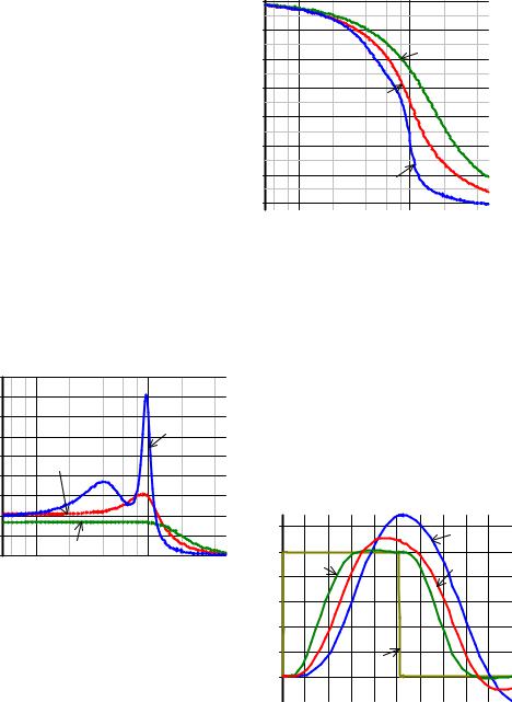
Let's now take a look at three filters. The nominal designs are identical; they all have two cascaded second-order Sallen & Key stages. But each filter has different R and C values.
Attenuation / db
0
-5
-10
-15
-20
-25
-30
100 |
200 |
400 |
1k |
2k |
4k |
10k |
20k |
40k |
100k |
Frequency / Hertz
Fig. 13-6: Frequency response of the filter in figure 13-5.
|
|
|
|
|
|
|
|
|
|
C4 |
|
|
|
|
|
|
|
|
|
|
|
|
|
|
|
C6 |
||||||
|
|
|
|
|
|
|
|
|
|
|
|
|
|
|
|
|
|
|
|
|
|
|
|
|
|
|
|
|
|
|
|
|
R7 |
|
|
R6 |
|
|
8.2n |
|
|
|
R11 |
|
R10 |
|
|
1.5n |
|||||||||||||||||
|
|
|
|
|
|
|
|
|
+ |
|
|
|
|
|
|
|
|
|
|
|
|
|
|
|
|
+ |
|
|
|
|
||
3.6k |
|
|
8.58k |
|
|
|
|
|
|
|
|
|
7.82k |
21.5k |
|
|
|
|
|
|
|
|
||||||||||
|
|
|
|
|
|
|
|
|
|
|
|
|
|
|
|
|
||||||||||||||||
|
|
|
1n |
|
|
|
|
|
|
|
|
|
|
|
|
|
|
|
1n |
|
|
|
|
|
|
|
|
|
|
|
||
|
|
|
|
|
|
|
|
|
|
|
|
|
|
|
|
|
|
C5 |
|
|
|
|
|
|
|
|
|
|
|
|||
|
|
|
C3 |
|
|
|
|
|
|
|
|
|
|
Sallen & Key |
|
|
|
|
|
|
|
|
|
|
|
|
|
|||||
|
|
|
|
|
|
|
|
|
|
|
|
|
|
|
Butterworth |
|
|
|
|
|
|
|
|
|
|
|
|
|
||||
|
|
|
|
|
|
|
|
|
|
|
|
|
|
|
|
|
|
|
|
|
|
|
|
|
|
|
|
|
|
|
|
|
|
|
C12 |
|
|
C2 |
|
R19 |
R18 |
1.5n |
R3 |
R 2 |
3.3n |
|
+ |
+ |
|||||
5.1k |
16.2k |
3.32k |
9.03k |
|||
|
|
|||||
|
1n |
|
|
1n |
|
|
|
|
|
C1 |
|
||
|
C11 |
|
Sallen & Key |
|
|
|
|
|
|
Bessel |
|
|
|
|
|
C13 |
|
|
C15 |
|
R22 |
R23 |
10n |
R26 |
R27 |
4.7n |
|
+ |
+ |
|||||
9.76k |
34.1k |
8.83k |
27.5k |
|||
|
|
|||||
|
82p |
|
|
1n |
|
|
|
|
|
C16 |
|
||
|
C14 |
|
Sallen & Key |
|
|
|
|
|
|
Chebyshev |
|
|
Fig. 13-7: Three fourth-order low-pass filters. The different component values result in different frequency responses.
|
0 |
|
|
|
|
|
|
|
-5 |
|
|
|
|
Bessel |
|
|
Chebyshev |
|
|
|
|
||
|
|
|
|
|
|
||
|
-10 |
|
|
|
|
|
|
|
-15 |
|
|
Butterworth |
|
|
|
|
|
|
|
|
|
|
|
dB |
-20 |
|
|
|
|
|
|
|
|
|
|
|
|
|
|
|
-25 |
|
|
|
|
|
|
|
-30 |
|
|
|
|
|
|
|
-35 |
|
|
|
|
|
|
|
-40 |
1k |
2k |
4k |
10k |
20k |
40k |
|
|
||||||
Frequency / Hertz
Fig. 13-8: Frequency responses of the three low-pass filters.
Judging by the frequency response alone, the Chebyshev filter has the sharpest response, though it produces some ripples in the pass-band (i.e. below 10kHz). This ripple can be reduced, at the expense of steepness above 10kHz. In even-order Chebyshev filters the ripples are above the line (0dB in this case); in oddorder ones they are below the line.
The Bessel filter gives a gentle roll-off with no overshoot in the pass-band, and the performance of the Butterworth filter is in between the other two.
Preliminary Edition September 2004 |
13-3 |
All rights reserved |
Camenzind: Designing Analog Chips |
Chapter 13: Filters |
µSecs
But there is more to the
performance of a filter than just |
0 |
|
|
|
|
|
the frequency response. Take |
-50 |
|
|
|
|
|
the phase of the signal, for |
|
|
|
|
|
|
|
|
|
|
Bessel |
|
|
example. It never stays |
|
|
|
|
|
|
-100 |
|
|
|
|
|
|
constant in any filter with the |
-150 |
|
|
|
|
|
delays caused by the |
|
|
|
|
|
|
deg |
Butterworth |
|
|
|
||
capacitors. But there is a |
|
|
|
|
|
|
-200 |
|
|
|
|
|
|
|
|
|
|
|
|
|
difference between the three |
-250 |
|
|
|
|
|
filter types. The Bessel filter |
|
|
|
|
|
|
|
|
|
|
|
|
|
has the smallest phase-shift, the |
-300 |
|
Chebyshev |
|
|
|
|
|
|
|
|
||
Chebyshev the largest. |
-350 |
|
|
|
|
|
The phase response |
1k |
2k |
4k |
10k |
20k |
40k |
|
|
|
|
|
|
|
influences two more measures |
Frequency / Hertz |
|
|
|
|
|
|
|
|
|
|
|
|
of filter quality. The first one is |
Fig. 13-9: Phase response of the three |
|||||
called Group Delay, shown in |
|
|
filters. |
|
|
|
|
|
|
|
|
|
|
figure 13-10. Assume that you pass through the filter not just one frequency, but several. A delay in the filter causes the phase-relationships of the different frequencies to change and distortion results.
The Bessel filter is by far the
180 |
|
best in this respect, having not only |
160 |
|
the shortest delay but also the most |
|
constant. The Chebyshev filter is by |
|
140 |
|
|
120 |
Chebyshev |
far the wildest. |
|
||
|
Also, we can judge a filter by |
|
Butterworth |
|
|
100 |
|
|
80 |
|
its pulse response. In figure 13-11 a |
|
|
|
60 |
|
|
40 |
|
|
|
|
|
|
|
|
|
|
|
|
|
|
|
|
|
|
|
|
|
|
|
|
1.2 |
|
|
|
|
|
|
|
Chebyshev |
||
20 |
|
Bessel |
|
|
|
|
|
|
|
|
|
|
|
|
|||
0 |
|
|
|
|
|
1 |
|
|
|
|
|
|
|
|
|
||
1k |
2k |
4k |
10k |
20k |
40k |
Bessel |
|
|
|
|
|
|
|
||||
|
|
|
|
|
|
Butterworth |
|||||||||||
|
|
|
|
|
|
|
|||||||||||
|
|
|
|
|
|
|
|
|
|
|
|
|
|||||
|
Frequency / Hertz |
|
|
|
|
0.8 |
|
|
|
|
|
|
|
|
|
||
Fig. 13-10: Group delay of the three filters. |
0.6 |
|
|
|
|
|
|
|
|
|
|||||||
|
|
|
|
|
|
|
V |
|
|
|
|
|
|
|
|
|
|
100usec pulse was applied to the |
|
0.4 |
|
|
|
|
|
|
|
|
|
||||||
|
|
|
|
|
|
|
|
|
|
|
|||||||
input. We expect a rounding of |
|
0.2 |
|
|
|
Input |
|
|
|
|
|
||||||
the corners at the output but, |
|
|
|
|
|
|
|
|
|
|
|||||||
|
0 |
|
|
|
|
|
|
|
|
|
|||||||
considering that all three filters |
|
0 |
20 |
40 |
60 |
80 |
100 |
120 |
140 |
160 |
180 |
||||||
have the same cut-off frequency, |
|
||||||||||||||||
|
Time/µSecs |
|
|
|
|
|
20µSecs/div |
||||||||||
the Bessel filter does the best job. |
|
|
|
|
|
||||||||||||
Fig. 13-11: Pulse response of the three |
|||||||||||||||||
|
|
|
|
|
|
|
|||||||||||
|
How do we get the values for |
|
|
|
|
filters. |
|
|
|
|
|||||||
|
|
|
|
|
|
|
|
|
|
|
|||||||
the resistors and capacitors? If you open up a text-book on filters, you will |
|||||||||||||||||
Preliminary Edition September 2004 |
13-4 |
All rights reserved |

Camenzind: Designing Analog Chips |
Chapter 13: Filters |
see elaborate tables giving you coefficients for Butterworth, Bessel and Chebyshev functions. This is no longer necessary. There are a multitude of programs available on the web (many of them at no cost), which calculate these values for you. Search for "active filter software".
Bessel, Chebyshev and Butterworth
Friedrich Wilhelm Bessel (1784 to 1846) was a professor of astronomy at the University of Königsberg in Germany. By measuring the position of some 50,000 stars he greatly advanced the state of celestial mechanics and came up with the Bessel function, which was found to be also useful in filters.
Pafnuty Chebyshev (1821 to 1894) taught mathematics at the University of St. Petersburg. His major contribution was the theory of prime numbers but, similar to Bessel he left behind a function which later turned out to be applicable to filters.
Of Stephen Butterworth we know only that he worked at the British Admiralty for almost all his life. In 1930 he published a paper "On the Theory of Filters". He died in 1958.
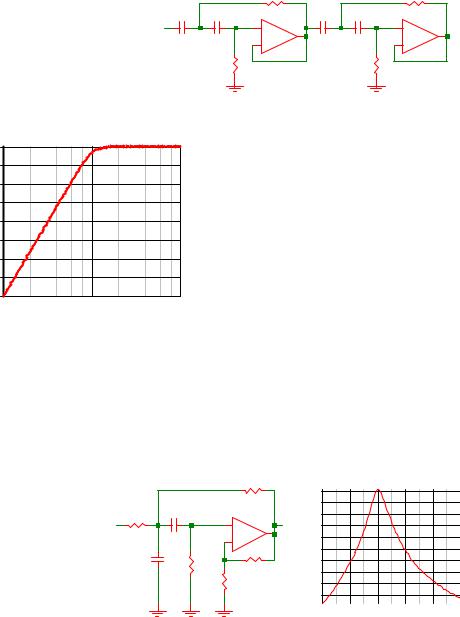
Let's look at two more low-pass filters, using designs other than Sallen & Key. The two stages in figure 13-12 use voltage-controlled voltagesources (VCVS), an approach differing from Sallen & Key only in that the op-amps have gain.
|
|
C2 |
|
|
C4 |
|
R1 |
R2 |
1.08n |
R5 |
R6 |
1n |
|
+ |
+ |
|||||
11.76k |
11.76k |
12.24k |
12.24k |
|||
|
|
|||||
|
C1 |
R3 |
|
C3 |
R7 |
|
|
1n |
1 k |
|
1n |
10k |
|
|
R4 |
|
R8 |
|||
|
|
9.5k |
|
|
8.1k |
Fig. 13-12: 4th-order low-pass Butterworth filter in a voltage-controlled voltage-source design.
|
|
|
|
|
|
|
|
|
|
|
|
|
|
|
|
|
|
|
|
|
|
|
|
|
|
|
|
|
|
|
|
|
|
|
The design |
|||||||||||
|
|
|
|
|
|
|
R 2 |
|
|
|
|
C2 |
|
|
|
|
|
|
|
R6 |
|
|
|
|
C3 |
|
||||||||||||||||||||
|
|
|
|
|
|
|
|
|
|
|
|
|
|
|
|
|
||||||||||||||||||||||||||||||
|
|
|
|
|
|
|
|
|
|
|
|
|
|
|
|
|
|
|
|
|
|
|
|
|
|
|
|
|
|
|
|
|
|
|
|
approach for each stage |
||||||||||
|
|
|
|
|
|
|
15k |
|
|
|
|
1n |
|
|
|
|
|
|
|
6.2k |
|
|
|
|
1n |
|
||||||||||||||||||||
|
|
|
|
|
|
|
|
|
|
|
|
|
||||||||||||||||||||||||||||||||||
R 1 |
|
|
|
|
|
|
|
R3 |
|
|
|
|
|
|
|
|
|
|
|
|
|
|
R5 |
|
|
|
|
R4 |
|
|
|
|
|
|
|
|
|
|
|
|
of figure 13-13 is |
|||||
|
|
|
|
|
|
|
|
|
|
|
|
|
|
|
|
|
|
|
|
|
|
|
|
|||||||||||||||||||||||
15k |
|
|
|
|
|
7.5k |
|
|
|
|
|
|
|
|
|
+ |
|
|
|
6.2k |
|
|
|
3.1k |
|
|
|
|
|
|
|
|
+ |
|
||||||||||||
|
|
|
|
|
|
|
|
|
|
|
|
|
|
|
|
|
|
|
|
|
|
|
|
|
|
|
|
|
||||||||||||||||||
|
|
|
|
|
|
|
|
|
|
|
|
|
|
|
|
|
|
|
|
|
|
|
|
|
|
|
|
|
||||||||||||||||||
|
|
|
|
|
|
|
|
|
|
|
|
|
|
|
|
|
|
|
|
|
|
|
|
|
|
|
|
|
|
|
|
|
|
|
|
|
|
|
|
|
|
|
|
called Multiple |
||
|
|
|
|
|
|
|
|
C1 |
|
|
|
|
|
|
|
|
|
|
|
|
|
|
|
|
|
|
|
C4 |
|
|
|
|
|
|
|
|
|
|
||||||||
|
|
|
|
|
|
|
|
|
|
|
|
|
|
|
|
|
|
|
|
|
|
|
|
|
|
|
|
|
|
|
|
|
||||||||||||||
|
|
|
|
|
|
|
|
2.7n |
|
|
|
|
|
|
|
|
|
|
|
|
|
|
|
|
|
|
|
15n |
|
|
|
|
|
|
|
|
|
|
Feedback. |
|||||||
|
|
|
|
|
|
|
|
|
|
|
|
|
|
|
|
|
|
|
|
|
|
|
|
|
|
|
|
|
|
|
|
|
|
|
|
|
||||||||||
|
|
|
|
|
|
|
|
|
|
|
|
|
|
|
|
|
|
|
|
|
|
|
|
|
|
|
|
|
|
|
|
|
|
|||||||||||||
|
|
|
|
|
|
|
|
|
|
|
|
|
|
|
|
|
|
|
|
|
|
|
|
|
|
|
|
|
|
|
|
|
|
|
|
|
|
|
|
|
|
|
|
|
|
|
|
|
|
|
|
|
|
|
|
|
|
|
|
|
|
|
|
|
|
|
|
|
|
|
|
|
|
|
|
|
|
|
|
|
|
|
|
|
|
|
|
|
|
|
|
|
All these |
|
|
|
|
|
|
|
|
|
|
|
|
|
|
|
|
|
|
|
|
|
|
|
|
|
|
|
|
|
|
|
|
|
|
|
|
|
|
|
|
|
|
|
|
|
|
|
|
|
|
|
|
|
|
|
|
|
|
|
|
|
|
|
|
|
|
|
|
|
|
|
|
|
|
|
|
|
|
|
|
|
|
|
|
|
|
|
|
|
|
|
|
|
|
Fig. 13-13: A 4th-order Multiple Feedback approach. |
|
different approaches |
||||||||||||||||||||||||||||||||||||||||||||
|
|
|
|
|
|
|
|
|
|
|
|
|
|
|
|
|
|
|
|
|
|
|
|
|
|
|
|
|
|
|
|
|
|
|
|
|
|
|
|
|
|
|
|
|
|
render the same |
frequency and phase response, but they differ in sensitivity, i.e. how much component and op-amp parameter variations will influence filter performance. A temperature and Monte Carlo analysis reveals the merits.
Preliminary Edition September 2004 |
13-5 |
All rights reserved |
Camenzind: Designing Analog Chips |
Chapter 13: Filters |
High-Pass Filters
There is no mystery to converting a low-pass filter into a high-pass one: you simply exchange resistors and capacitors.
The drop-off now occurs toward the low-
|
|
R2 |
|
|
R 4 |
C 1 |
C 2 |
6.1k |
C3 |
C4 |
14.7k |
|
|
||||
|
|
+ |
|
|
+ |
1 n |
1 n |
|
1n |
1n |
|
|
R1 |
|
|
R 3 |
|
|
41.6k |
|
|
17.2k |
|
Fig. 13-14: High-pass Sallen & Key filter with Butterworth values.
|
0 |
|
|
|
|
|
|
|
-10 |
|
|
|
|
|
|
|
-20 |
|
|
|
|
|
|
|
-30 |
|
|
|
|
|
|
/ db |
-40 |
|
|
|
|
|
|
dB |
|
|
|
|
|
|
|
|
|
|
|
|
|
|
|
|
-50 |
|
|
|
|
|
|
|
-60 |
|
|
|
|
|
|
|
-70 |
|
|
|
|
|
|
|
1k |
2k |
4k |
10k |
20k |
40k |
100k |
Frequency / Hertz
Fig. 13-15: Frequency response of the 4th-order high-pass filter of figure 13-14.
frequency end, but at the same rate as that of a high-pass filter, 80dB per decade for a fourth-order filter.
Note that in all of these drawings, abstract op-amps are used (inside the symbol is an ideal voltagecontrolled voltage-source). In a practical design you have to consider the power supply. With a single supply, you may have to bias the input midway between ground and +V. In figure 13-14 this is accomplished at the low ends of R1 and R3.
Band-Pass Filters
Take the second-order low - pass filter of figure 13-5 and convert one RC network to high-pass. You now have a drop-off in amplitude at both
high and low frequencies.
|
|
|
|
R2 |
|
|
|
|
|
|
|
|
|
3.3k |
|
0 |
|
|
|
|
|
|
|
|
-2 |
|
|
|
|
|
|
|
|
|
|
|
|
|
|
R1 |
C2 |
|
|
|
|
-4 |
|
|
|
|
|
+ |
|
|
|
|
|
|
|
83.1k |
|
|
|
|
-6 |
|
|
|
|
1n |
|
|
|
/ db |
-8 |
|
|
|
|
|
|
|
|
|
|
|
|||
|
C1 |
|
|
R5 |
-10 |
|
|
|
|
|
R3 |
|
dB |
|
|
|
|||
|
|
|
|
|
|
||||
|
|
|
|
|
|
|
|||
|
|
|
|
|
-12 |
|
|
|
|
|
1n |
3.18k |
R4 |
10k |
|
-14 |
|
|
|
|
|
|
5k |
|
|
-16 |
|
|
|
|
|
|
|
|
|
-18 |
|
|
|
|
|
|
|
|
|
40 |
50 |
60 |
70 |
|
|
|
|
|
|
Frequency/kHertz |
|
|
10kHertz/div |
Fig. 13-16: Sallen & Key band- |
Fig. 13-17: Second-order |
pass filter. |
band-pass filter response. |
Preliminary Edition September 2004 |
13-6 |
All rights reserved |

Camenzind: Designing Analog Chips |
Chapter 13: Filters |
Although the arrangement is called a second-order band-pass filter, the drop-off rate is only first-order, 20dB per decade, since only one pole is active in each frequency segment. We can of course improve this by adding more stages, each stage contributing another 20dB per decade drop-off. And here there is a bewildering number of schemes available, with names such as Wien-Robinson, Deliyannis, Fliege, Twin-T, MikhaelBhattacharyya, Berka-Herpy and Akerberg-Mossberg. Your filter program will tell you which one to choose.
There is also an additional choice for the frequency response: compared to the Chebyshev filter the elliptic (or Cauer) has an even steeper initial drop-off, but the attenuation in the stop-band (i.e. outside the passband) is not flat.
R1 |
R2 |
|
|
R8 |
R9 |
|
|
+ |
|
6k |
12k |
+ |
|||
94.5k |
94.5k |
R6 |
|||||
|
|
|
|
||||
|
6.4k |
|
|
|
|||
C1 |
C3 |
|
C5 |
C6 |
|
||
|
|
|
|||||
30.9p |
3 3 p |
|
|
270p |
270p |
|
|
R3 |
66p |
R4 |
|
R 1 0 |
540p |
R11 |
|
47.2k |
220 |
|
6 k |
220 |
|||
|
C4 |
+ |
|
|
C7 |
+ |
|
|
|
|
R7 |
|
|||
|
|
|
|
|
|
||
2.1p |
|
R5 |
|
95.6k |
|
R12 |
|
|
|
|
|
||||
C2 |
|
34.9k |
|
|
|
34.9k |
Fig. 13-18: A fourth-order, twin-T elliptic band-pass filter.
The filter of figure 13-18 has two Twin-T stages. The first stage is |
|||||||||||
a second-order low -pass notch |
|
|
|
|
|
|
|
|
|
|
|
configuration, the second stage is |
|
10 |
|
|
|
|
|
|
|
|
|
called a second-order high-pass |
|
|
|
|
|
|
|
|
|
|
|
|
|
|
|
|
|
|
|
|
|
|
|
notch filter. The center frequency |
|
0 |
|
|
|
|
|
|
|
|
|
|
|
|
|
|
|
|
|
|
|
|
|
was chosen to be 50kHz, the |
db |
-10 |
|
|
|
|
|
|
|
|
|
bandwidth 2kHz. Just outside the |
/ |
|
|
|
|
|
|
|
|
|
|
dB |
|
|
|
|
|
|
|
|
|
||
|
|
|
|
|
|
|
|
|
|
||
|
|
|
|
|
|
|
|
|
|
|
|
bandwidth the attenuation reaches |
|
-20 |
|
|
|
|
|
|
|
|
|
a maximum, but then settles down |
|
|
|
|
|
|
|
|
|
|
|
to a modest 15dB. |
|
-30 |
|
|
|
|
|
|
|
|
|
|
|
|
|
|
|
|
|
|
|
|
|
|
|
4 2 |
44 |
4 6 |
48 |
50 |
5 2 |
54 |
5 6 |
58 |
6 0 |
It must be clear to you by |
Frequency/kHertz |
2kHertz/div |
|
Fig. 13-19: Response of a fourth-order |
|||
now that active filters are costly. |
|||
Not only do they require precision |
elliptic band-pass filter. |
|
|
|
|
||
components, but the values of most
capacitors and some of the resistors are such that they cannot be integrated. A fourth-order low-pass or high-pass filter requires at least eight external
Preliminary Edition September 2004 |
13-7 |
All rights reserved |
Camenzind: Designing Analog Chips |
Chapter 13: Filters |
components and five pins. For a band-pass filter with only modest performance 14 external components and pins are needed.
Switched Capacitor Filters
If we charge a capacitor (CR) by |
|
|
|
|
|
|
|
|
|
|
|
|
|
|
|
|
|
|
|
|
|
|
|
|
|
|
Clock |
|
closing switch S1 for a brief period of time, |
|
|
|
|
|
|
|
|
|
|
|
|
|
|
|
|
|
|
|
|
|
|
|
|
|
|
||
|
|
|
|
|
|
|
|
|
|
|
|
|
|
|
|
|
|
|
|
|
|
|
|
|
|
|
|
|
|
|
|
|
|
|
|
|
|
|
|
|
|
|
|
|
|
|
|
|
|
|
|
|
|
|
|
|
|
then open S1 and close S2 for the same |
|
|
|
|
|
|
|
|
|
|
|
|
|
|
|
|
|
|
|
|
|
|
|
|
|
|
|
|
|
|
|
|
|
|
|
|
|
|
|
|
|
|
|
|
|
|
|
|
|
|
|
|
|
|
|
|
|
|
|
|
|
|
|
|
|
|
|
|
|
|
|
|
|
|
|
|
|
|
|
|
|
|
|
|
|
|
amount of time, the potential across the |
|
|
|
|
|
|
|
|
|
|
|
|
|
|
|
|
|
|
|
|
|
|
|
|
|
|
|
|
|
|
|
|
|
|
|
|
|
|
|
|
|
|
|
|
|
|
|
|
|
|
|
|
|
|
|
|
|
capacitor is first that of V1, then V2. |
V1 |
|
|
|
|
|
|
|
|
|
|
|
|
|
|
|
|
|
|
|
|
|
|
|
|
|
|
V2 |
|
|
|
|
S1 |
|
|
|
|
S2 |
|||||||||||||||||||
One of the handiest formulae to carry |
|
|
|
|
|
|
|
|
|
|
|
|
|
CR |
||||||||||||||
|
|
|
|
|
|
|
|
|
|
|
|
|
||||||||||||||||
|
|
|
|
|
|
|
|
|
|
|
|
|
||||||||||||||||
in your mind is: |
|
|
|
|
|
|
|
|
|
|
|
|
|
|
|
|
|
|
|
|
|
|
|
|
|
|
|
|
|
|
|
|
|
|
|
|
|
|
|
|
|
|
|
|
|
|
|
|
|
|
|
|
|
|
|
|
|
Q = C V = I t |
|
|
|
|
|
|
|
|
|
|
|
|
|
|
|
|
|
|
|
|
|
|
|
|
|
|
|
|
|
Fig. 13-20: Making a resistor |
|||||||||||||||||||||||||||
|
|
|||||||||||||||||||||||||||
i.e. the charge in a capacitor (in Coulombs) |
|
|
|
out of a capacitor by |
||||||||||||||||||||||||
|
|
switching. at a rapid rate. |
||||||||||||||||||||||||||
is given by either the capacitance times the |
|
|
|
|
|
|
|
|
|
|
|
|
|
|
|
|
|
|
|
|
|
|
|
|
|
|
|
|
voltage or the current flowing into the capacitor for a certain period of time. In the case of figure 13-20, the current flowing between the two terminals over one period is
I = |
CR |
(V1 − V 2) |
= C (V1 |
− V 2) fclock |
|
tclock |
|||
|
|
|
|
If we had a resistor between V1 and V2 instead of the switches and the capacitor, the current flowing through it would be:
I = (V1 − V 2)
R
Thus the equivalent resistance of the switched capacitor is:
1
R =
CR fclock
Let's look at some numbers. Suppose the switching frequency is 100kHz and CR = 5pF:
R = |
1 |
|
= 2 10 6 |
= 2 MegOhms |
|
105 5 10 |
−12 |
||||
|
|
|
Preliminary Edition September 2004 |
13-8 |
All rights reserved |
Camenzind: Designing Analog Chips |
Chapter 13: Filters |
Thus, with a relatively small capacitor we can create the equivalent of a large-value resistor. If we were to implement such a device directly, the cost in area would be prohibitive.
But the area reduction is just the first benefit of switching; there is more: if we use this resistor in a filter, the absolute capacitance value disappears.
Shown here is a simple, one- |
|
|
|
|
|
|
|
|
|
|
|
|
|
|
|
|
|
|
|
|
|
|
|
|
|
|
|
|
|
|
Clock |
|||||
pole low -pass filter. The cutoff |
|
|
|
|
|
|
|
|
|
|
|
|
|
|
|
|
|
|
|
|
|
|
|
|
|
|
|
|
|
|
||||||
|
|
|
|
|
|
|
|
|
|
|
|
|
|
|
|
|
|
|
|
|
|
|
|
|
|
|
|
|
|
|
|
|
|
|||
frequency is given by: |
|
|
|
|
|
|
|
|
|
|
|
|
|
|
|
|
|
|
|
|
|
|
|
|
|
|
|
|
|
|
|
|
|
|
||
|
|
|
|
|
|
|
|
|
|
|
|
|
|
|
|
|
|
|
|
|
|
|
|
|
|
|
|
|
|
|
|
|
|
|||
|
|
|
|
|
|
|
|
|
|
|
|
|
|
|
|
|
|
|
|
|
|
|
|
|
|
|
|
|
|
|
|
|
|
|||
f3dB = |
1 |
|
|
|
|
|
|
|
|
|
|
|
|
|
|
|
|
|
|
|
|
|
|
|
|
|
|
|
|
|
|
|
|
|
|
|
|
|
|
|
|
|
|
|
|
|
|
|
|
|
|
|
|
|
|
|
|
|
|
|
|
|
|
|
|
|
|
|
|
|
|
||
|
|
|
|
|
|
|
|
|
|
|
|
|
|
|
|
|
|
|
|
|
|
|
|
|
|
|
|
|
|
|
|
|
|
|
||
|
|
|
|
|
|
|
S1 |
|
|
|
|
|
|
|
|
|
|
S2 |
|
|
||||||||||||||||
|
|
|
|
|
|
|
|
|
|
|
|
|
|
|
|
|
|
|
||||||||||||||||||
2π R C |
|
|
|
|
|
|
|
|
|
|
||||||||||||||||||||||||||
|
|
|
|
|
|
|
|
|
|
|
|
|
|
|
|
|
|
|
|
|
|
|
|
|
|
|
|
|
|
|
|
|
|
|||
|
|
|
|
|
|
|
|
|
|
|
|
|
|
|
|
|
CR |
|
|
|
|
|
|
|
|
|
|
|
|
|
|
|
C |
|||
|
|
|
|
|
|
|
|
|
|
|
|
|
|
|
|
|
|
|
|
|
|
|
|
|
|
|
|
|
|
|
||||||
|
|
|
|
|
|
|
|
|
|
|
|
|
|
|
|
|
|
|
|
|
|
|
|
|
|
|
|
|
|
|
|
|
|
|
|
|
|
|
|
|
|
|
|
|
|
|
|
|
|
|
|
|
|
|
|
|
|
|
|
|
|
|
|
|
|
|
|
|
|
|
|
|
|
Substituting the equivalent resistance of the switched capacitor we get:
f3dB |
= |
f clock C |
|
2π CR |
|||
|
|
R
If we make the two capacitors equal (any value) and switch at a rate of 100kHz we get a filter with a cutoff frequency of 15.9kHz. If CR is ten times the size of C and the clock
frequency remains at 100kHz, the cutoff frequency decreases to 1.59kHz. Thus, the switched-capacitor filter has two significant advantages
over the active (linear) one:
1.A low cutoff frequency can be achieved with capacitor values small enough to allow integration.
2.The cutoff frequency is not influenced by absolute variations. Given an accurate clock frequency and capacitor ratios of 1%, the cutoff frequency will be within 1%.
The simple low-pass filter can be expanded into any of the configuration discussed under active filters. Take for example the Sallen & Key filters in figure 13-7. In a switched-capacitor design you would first
Preliminary Edition September 2004 |
13-9 |
All rights reserved |
Camenzind: Designing Analog Chips |
Chapter 13: Filters |
greatly reduce the values of the capacitors and then replace the resistors with a capacitor and switches.
The switched-capacitor filter requires lateral switches, which are easily implemented in CMOS, but cumbersome (and slow) in a bipolar process. For this reason, this approach has become exclusively CMOS
territory. |
|
|
|
|
|
|
|
|
|
|
|
|
|
|
|
To minimize the influence of stray |
|
Ph1 |
|
|
|
|
|
|
|
|
Ph2 |
||||
capacitances four (CMOS) switches are |
|
|
|
|
|
|
CR |
||||||||
|
|
|
|
|
|
|
|
|
|
|
|
|
|
|
|
often used instead of two, resulting in an |
|
|
|
|
|
|
|
|
|
|
|
|
|
|
|
inverting configuration. |
|
Ph2 |
|
|
|
|
|
|
|
Ph1 |
|||||
For either switch design it is |
|
|
|
|
|
|
|
|
|
|
|
|
|
|
|
|
|
|
|
|
|
|
|
|
|
|
|
|
|
|
|
important that the two lateral switches |
|
|
|
|
|
|
|
|
|
|
|
|
|
|
|
|
|
|
|
|
|
|
|
|
|
|
|
|
|
|
|
never be closed at the same time, i.e. there |
|
Fig. 13-22: Switch |
|||||||||||||
must be some "dead-time" between the |
configuration to minimize |
||||||||||||||
two phases of the clock. |
|
the effect of stray |
|||||||||||||
capacitances in CMOS. |
|||||||||||||||
There are three disadvantages with switched-capacitor filters:
1.No matter how carefully you design the switches, there is always some switching noise.
2.A switched-capacitor filter samples the signal. To get an adequate sample, the highest signal frequency cannot exceed about 10% of the clock frequency. If there are signals present above that point, the switchedcapacitor filter will produce a mixture of new frequencies, some of which may appear in the 0 to 10% frequency range. To avoid such false signals, a linear (active) filter must be used at the input (an anti-aliasing filter).
3.A switched-capacitor filter can only be simulated in real time, i.e. with a transient analysis; you cannot take advantage of the many features of an AC analysis, such as measuring frequency and phase response. And with the clock frequency necessarily being high, simulation takes far more time compared to an active filter.
4.The output has sampled noise, which is present even if the input is zero.
Preliminary Edition September 2004 |
13-10 |
All rights reserved |

Camenzind: Designing Analog Chips |
Chapter 14: Power |
14 Power
Linear Regulators
Let's say you have 12 Volts available but need 3.3. Your 3.3-Volt load consumes up to 500mA. The 12-Volt source (e.g. a car battery) fluctuates between 10 and 14 Volts; the lower voltage needs to be within 5%.
The immediate choice to effect this change in voltage is a linear regulator. Look at it as a variable resistor, dropping whatever voltage is not needed.
|
Q1 |
|
|
|
|
Vcc |
|
|
|
|
|
|
|
|
|
|
|
|
Q9 |
|
|
|
|
|
|
|
Q12 |
Q 2 |
Repi |
|
Q7 |
C 1 |
|
Q13 |
|
|
|
|
|
|
|
|
|
|
|
10p |
|
5 0 |
|
|
|
|
|
|
|
|
|
|
Q15 |
|
|
Vreg |
|
|
|
|
Q10 |
R3 |
|
|
|
Q14 |
|
|
||
|
|
|
|
|
||
|
|
|
|
|
26.25k |
|
|
|
|
|
|
|
|
|
R1 |
|
Q5 |
Q6 |
|
|
|
3k |
|
|
|
||
|
|
|
|
|
|
|
|
Q3 |
|
|
|
|
R4 |
|
Q16 |
|
|
|
15k |
|
|
|
|
|
|
||
Q4 |
|
|
Q8 |
|
|
|
|
|
|
|
|
|
|
|
R2 |
|
Vref |
|
|
|
|
6k |
|
|
Q11 |
|
|
|
|
|
|
|
|
|
|
|
|
1.2 |
|
|
SUB |
|
|
|
|
|
|
The unwanted voltage is dropped in an NPN transistor. In figure 14-1 this is a Darlington configuration to minimize the drive current; it requires at least 2.2 Volts difference between Vcc and Vreg, but it is an easy and simple design.
The regulator uses a 1.2-Volt bandgap reference
(see chapter 7), whose voltage is compared with a fraction of the regulated output by the differential amplifier Q5, Q6, Q7 and Q10. Once the circuit is in balance the voltages at the bases of Q5 and Q6 are equal, so the regulated voltage is:
Vreg = Vref ( R3 + R4)
R4
Preliminary Edition September 2004 |
14-1 |
All rights reserved |
Camenzind: Designing Analog Chips |
Chapter 14: Power |
An operating current is set up by Q1 to Q4 ( a circuit derived from figure 5-4) and mirrored by Q9. At this point we have about 150uA and the current has a deliberate negative temperature coefficient (R2, which creates this current, is connected across a VBE, which itself has a negative tempco). This counteracts the positive tempco of hFE.
Q10 shunts to ground whatever operating current is not needed by the output stage.
Using a Darlington
configuration for the output |
|
|
|
|
|
|
|
3.5 |
|
|
|
|
|
|
|
|
|
|
|
|
|
|
|
|
|
|
|
|
|||||||||||
greatly reduces the required |
|
|
|
|
|
|
|
3 |
|
|
|
|
|
|
|
|
|
|
|
|
|
|
|
|
|
|
|
|
|||||||||||
|
|
|
|
|
|
|
|
|
|
|
|
|
|
|
|
|
|
|
|
|
|
|
|
|
|
|
|||||||||||||
|
|
|
|
|
|
|
|
|
|
|
|
|
|
|
|
|
|
|
|
|
|
|
|
|
|
|
|||||||||||||
|
|
|
|
|
|
|
|
|
|
|
|
|
|
|
|
|
|
|
|
|
|
|
|
|
|
|
|
|
|||||||||||
operating current, but there must |
|
|
|
2.5 |
|
|
|
|
|
|
|
|
|
|
|
|
|
|
|
|
|
|
|
|
|||||||||||||||
|
|
|
|
|
|
|
|
|
|
|
|
|
|
|
|
|
|
|
|
|
|
|
|||||||||||||||||
always be a substantial voltage |
|
/ V |
|
|
|
|
|
|
|
|
|
|
|
|
|
|
|
|
|
|
|
|
|
|
|||||||||||||||
|
|
|
|
|
|
|
|
|
|
|
|
|
|
|
|
|
|
|
|
|
|
||||||||||||||||||
drop between supply and output. |
|
Voltage |
2 |
|
|
|
|
|
|
|
|
|
|
|
|
|
|
|
|
|
|
|
|
||||||||||||||||
|
|
|
|
|
|
|
|
|
|
|
|
|
|
|
|
|
|
|
|
|
|||||||||||||||||||
|
|
|
|
|
|
|
|
|
|
|
|
|
|
|
|
|
|
|
|
|
|
|
|||||||||||||||||
For this reason such a circuit is |
|
|
|
|
|
|
|
|
|
|
|
|
|
|
|
|
|
|
|
|
|
|
|
||||||||||||||||
|
Output |
1.5 |
|
|
|
|
|
|
|
|
|
|
|
|
|
|
|
|
|
|
|
|
|||||||||||||||||
|
|
|
|
|
|
|
|
|
|
|
|
|
|
|
|
|
|
|
|
|
|||||||||||||||||||
|
|
|
|
|
|
|
|
|
|
|
|
|
|
|
|
|
|
|
|
|
|
|
|||||||||||||||||
anything but a low-dropout |
|
|
|
|
|
1 |
|
|
|
|
|
|
|
|
|
|
|
|
|
|
|
|
|
|
|
|
|||||||||||||
|
|
|
|
|
|
|
|
|
|
|
|
|
|
|
|
|
|
|
|
|
|
|
|
|
|
|
|||||||||||||
regulator. For our application, a |
|
|
|
|
|
|
|
|
|
|
|
|
|
|
|
|
|
|
|
|
|
|
|
||||||||||||||||
|
|
|
|
|
|
|
|
|
|
|
|
|
|
|
|
|
|
|
|
|
|
|
|
|
|||||||||||||||
|
|
|
|
|
|
|
|
|
|
|
|
|
|
|
|
|
|
|
|
|
|
|
|
|
|||||||||||||||
conversion from 10 Volts min. to |
|
|
|
0.5 |
|
|
|
|
|
|
|
|
|
|
|
|
|
|
|
|
|
|
|
|
|||||||||||||||
|
|
|
|
|
|
|
|
|
|
|
|
|
|
|
|
|
|
|
|
|
|
|
|||||||||||||||||
|
|
|
|
|
|
|
|
|
|
|
|
|
|
|
|
|
|
|
|
|
|
|
|
|
|||||||||||||||
3.3 Volts this is of little concern. |
|
|
|
0 |
|
|
|
|
|
|
|
|
|
|
|
|
|
|
|
|
|
|
|
|
|||||||||||||||
|
|
|
0 |
2 |
4 |
6 |
|
8 |
|
10 |
12 |
||||||||||||||||||||||||||||
|
The current that flows |
|
|
|
|
|
|
|
|
|
|
Supply Voltage/V |
|
|
|
|
|
|
|
|
|
|
|
2V/div |
|||||||||||||||
through the load also flows |
|
|
|
|
|
|
|
|
|
|
|
Fig. 14-2: Drop-out voltage of NPN |
|||||||||||||||||||||||||||
through the output transistor. So, at |
|
|
|
|
|
|
|
|
|
regulator. |
|
|
|
|
|
|
|
|
|||||||||||||||||||||
500mA, the load consumes 1.65 |
|
|
|
|
|
|
|
Watts, the regulator 4.36 Watts |
|||||||||||||||||||||||||||||||
|
4.5 |
|
|
|
|
|
|
|
|
|
|
|
|
|
|
|
|
|
|
|
|
||||||||||||||||||
|
|
|
|
|
|
|
|
|
|
|
|
|
|
|
|
|
|
|
|
|
(with 12-Volts in), which is |
||||||||||||||||||
|
|
|
|
|
|
|
|
|
|
|
|
|
|
|
|
|
|
|
|
|
|||||||||||||||||||
|
4 |
|
|
|
|
|
|
|
|
|
|
|
|
|
|
|
|
|
|
|
|
||||||||||||||||||
|
|
|
|
|
|
|
|
|
|
|
|
|
|
|
|
|
|
|
|
|
simply converted into heat. |
||||||||||||||||||
|
3.5 |
|
|
|
|
|
|
|
|
|
|
|
|
|
|
|
|
|
|
|
|
||||||||||||||||||
W |
|
|
|
|
|
Output |
Transistor |
|
|
|
|
|
|
|
|
|
|
This the main disadvantage of |
|||||||||||||||||||||
|
|
|
|
|
|
|
|
|
|
|
|
|
|
|
|
||||||||||||||||||||||||
/ |
|
|
|
|
|
|
|
|
|
|
|
|
|
|
|
|
|
|
|
|
|
|
|
|
|
|
|
|
|
|
|
|
|
|
|
|
|
|
|
Dissipation |
3 |
|
|
|
|
|
|
|
|
|
|
|
|
|
|
|
|
|
|
|
|
a linear regulator. The heat is |
|||||||||||||||||
2.5 |
|
|
|
|
|
|
|
|
|
|
|
|
|
|
|
|
|
|
|
|
|||||||||||||||||||
|
|
|
|
|
|
|
|
|
|
|
|
|
|
|
|
|
|
|
|
produced mainly by one |
|
|
|
||||||||||||||||
2 |
|
|
|
|
|
|
|
|
|
|
|
|
|
|
|
|
|
|
|
|
|
|
|
||||||||||||||||
|
|
|
|
|
|
|
|
|
|
|
|
|
|
|
|
|
|
|
|
device: Q13. Thus there will |
|||||||||||||||||||
Power |
1.5 |
|
|
|
|
|
|
|
|
|
|
|
|
|
|
|
|
|
|
|
|
||||||||||||||||||
|
|
|
|
|
|
|
|
|
|
|
|
|
|
|
|
|
|
|
|
be a hot-spot on the chip and |
|||||||||||||||||||
|
|
|
|
|
|
|
|
|
|
Load |
|
|
|
|
|
|
|||||||||||||||||||||||
|
|
|
|
|
|
|
|
|
|
|
|
|
|
|
|
|
|||||||||||||||||||||||
|
1 |
|
|
|
|
|
|
|
|
|
|
|
|
|
|
|
|
||||||||||||||||||||||
|
|
|
|
|
|
|
|
|
|
|
|
|
|
|
|
|
|
|
|
|
resulting temperature |
|
|
|
|
|
|||||||||||||
|
0.5 |
|
|
|
|
|
|
|
|
|
|
|
|
|
|
|
|
|
|
|
|
|
|
|
|
|
|||||||||||||
|
|
|
|
|
|
|
|
|
|
|
|
|
|
|
|
|
|
|
|
|
gradients, even with an |
|
|
|
|
|
|||||||||||||
|
0 |
|
|
|
|
|
|
|
|
|
|
|
|
|
|
|
|
|
|
|
|
|
|
|
|
|
|||||||||||||
|
|
|
|
2 |
4 |
6 |
|
8 |
|
|
10 |
|
12 |
|
|
adequate heat-sink. These |
|
|
|
||||||||||||||||||||
|
0 |
|
|
|
|
|
|
|
|
|
|
||||||||||||||||||||||||||||
|
|
|
|
|
|
|
|
|
|
|
|
|
|
|
|
|
|
|
|
|
|
|
|
|
|||||||||||||||
|
|
|
Supply Voltage/V |
|
|
|
|
|
|
|
|
2V/div |
temperature gradients are |
|
|
|
|||||||||||||||||||||||
|
|
|
|
|
|
|
|
|
|
|
|
|
|
|
|
|
|
|
|
|
|
|
|
|
|||||||||||||||
Fig. 14-3: In a linear regulator the energy not |
|
|
|
|
bound to influence other |
|
|
|
|||||||||||||||||||||||||||||||
|
required by the load is converted into heat. |
|
|
|
|
circuitry on the chip, including |
|||||||||||||||||||||||||||||||||
|
|
|
|
|
|
|
|
|
|
|
|
|
|
|
|
|
|
|
|
|
|
the regulator's own reference |
|||||||||||||||||
A linear regulator with an NPN output transistor is relatively easy the compensate. Despite the fact that the loop gain is high (which results in an output impedance of a mere 4mOhm) the circuit is rendered stable with a
Preliminary Edition September 2004 |
14-2 |
All rights reserved |