

Verilog
assign QX = (LD == 1'b1) ? INCR : D; assign INCR = Q + 8'h01;
always @(posedge CLK or posedge RST) if (RST == 1’b1)
Q = 8’b0 ; else
Q = QX ; endmodule
module PREP2_COMP ( A, B, EQ); input [7:0] A, B;
output EQ;
assign EQ = (A == B); endmodule
module TOP_LEVEL ( CLK, RST, SEL, LDCOMP, LDPRE, DATA1, DATA2, DATA0);
input CLK, RST, SEL, LDCOMP, LDPRE; input [7:0] DATA1, DATA2;
output [7:0] DATA0;
wire [7:0] QPRE, QCOMP, QX, YX; wire LD;
PREP2_REG ONE (CLK, RST, LDPRE, DATA2, QPRE); PREP2_REG TWO (CLK, RST, LDCOMP, DATA2, QCOMP); PREP2_COUNT THREE (CLK, RST, LD, YX, QX); PREP2_COMP FOUR (QX, QCOMP, LD);
assign YX = (SEL == 1'b0) ? DATA1 : QPRE; assign DATA0 = QX;
endmodule
Figure 52: Complete Verilog representation of the 8-bit timer/counter
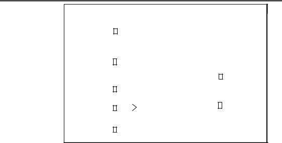
5.2. Example 2: memory map (prepbenchmark 9)
Example 2 implements a memory mapped I/O scheme of different sized memory spaces common to microprocessor systems.
Addresses are decoded when the address strobe (AS) is active according to an address space and each space has an output indicating that it is active. Addresses that fall outside the boundary of the decoder active a bus error (BE) signal.
Figure 53 represents the block diagram of this example. Figure 54 gives the outputs value according to the inputs value and figure 55 gives the Verilog description.
Verilog - 27
Verilog
|
|
|
|
|
|
|
H |
Q7 |
|
|
|
|
|
|
|
|
|
|
Q6 |
|
|
|
|
AH |
|
|
|
A[15:8] |
|
G |
|
|
|
||
|
|
|
|
|
|
|
|||||
|
Q5 |
|
|
|
|||||||
|
|
|
|
|
|
||||||
|
|
|
|
|
|
|
|||||
|
|
|
|
|
|
|
F |
|
|
|
|
|
|
|
|
|
|
|
Q4 |
|
|
|
|
|
|
|
|
|
|
|
E |
|
|
|
|
|
|
|
|
|
|
|
Q3 |
|
|
|
|
|
|
|
|
|
|
|
D |
|
|
|
|
|
|
|
|
|
|
|
|
|
|
|
|
AL |
|
|
|
|
A[7:0] |
|
C |
Q2 |
|
|
|
|
|
|
|
|
|
|
|
||||
|
|
|
|
Q1 |
|
|
|
||||
|
|
|
|
|
|
||||||
|
|
|
|
|
|
|
B |
|
|
|
|
|
|
|
|
|
|
|
Q0 |
|
|
Q |
|
AS |
|
|
|
|
ADDRESS |
A |
|
|
|||
|
|
|
|
|
|
||||||
|
|
|
|
|
|||||||
|
|
|
|
|
|
||||||
|
|
|
|
|
|
|
|
|
|||
|
|
|
STROBE |
|
|
|
|
|
|||
|
|
|
|
|
|
|
|||||
|
|
|
|
|
|
|
|
||||
|
|
|
|
|
|
|
|
|
|
||
CLK |
|
|
|
|
CLK |
|
BUS |
|
|
|
BE |
|
|
|
|
|
|
|
|
||||
|
|
|
|
ERROR |
|
|
|
||||
|
|
|
|
|
|
||||||
|
|
|
|
|
|
|
|||||
|
|
|
|
|
|
|
|
|
|
||
|
|
|
|
|
RST |
|
|
|
|
|
|
RST |
|
|
|
|
|
|
|
|
|
|
|
|
|
|
|
|
|
|
|
|
|
||
|
|
|
|
|
|
|
|
|
|||
Figure 53: Example 2: a memory map
RST |
AS |
CL |
AH & AL |
A |
B |
C |
D |
E |
F |
G |
|
H |
BE |
|
|
K |
|
|
|
|
|
|
|
|
|
|
|
|
|
|
|
|
|
|
|
|
|
|
|
|
|
1 |
X |
X |
X |
0 |
0 |
0 |
0 |
0 |
0 |
0 |
|
0 |
0 |
0 |
0 |
¤ |
X |
0 |
0 |
0 |
0 |
0 |
0 |
0 |
|
0 |
0 |
0 |
X |
* |
X |
A B C D E F G H BE |
|||||||||
|
|
|
|
|
|
|
|
|
|
|
|
|
|
0 |
1 |
¤ |
FFFF to |
1 |
0 |
0 |
0 |
0 |
0 |
0 |
|
0 |
0 |
|
|
|
F000 |
|
|
|
|
|
|
|
|
|
|
|
|
|
|
|
|
|
|
|
|
|
|
|
|
0 |
1 |
¤ |
EFFF to |
0 |
1 |
0 |
0 |
0 |
0 |
0 |
|
0 |
0 |
|
|
|
E800 |
|
|
|
|
|
|
|
|
|
|
|
|
|
|
|
|
|
|
|
|
|
|
|
|
0 |
1 |
¤ |
E7FF to |
0 |
0 |
1 |
0 |
0 |
0 |
0 |
|
0 |
0 |
|
|
|
E400 |
|
|
|
|
|
|
|
|
|
|
|
|
|
|
|
|
|
|
|
|
|
|
|
|
0 |
1 |
¤ |
E3FF to |
0 |
0 |
0 |
1 |
0 |
0 |
0 |
|
0 |
0 |
|
|
|
E300 |
|
|
|
|
|
|
|
|
|
|
|
|
|
|
|
|
|
|
|
|
|
|
|
|
0 |
1 |
¤ |
E2FF to |
0 |
0 |
0 |
0 |
1 |
0 |
0 |
|
0 |
0 |
|
|
|
E2C0 |
|
|
|
|
|
|
|
|
|
|
|
|
|
|
|
|
|
|
|
|
|
|
|
|
0 |
1 |
¤ |
E2BF to |
0 |
0 |
0 |
0 |
0 |
1 |
0 |
|
0 |
0 |
|
|
|
E2B0 |
|
|
|
|
|
|
|
|
|
|
|
|
|
|
|
|
|
|
|
|
|
|
|
|
0 |
1 |
¤ |
E2AF to |
0 |
0 |
0 |
0 |
0 |
0 |
1 |
|
0 |
0 |
|
|
|
E2AC |
|
|
|
|
|
|
|
|
|
|
|
|
|
|
|
|
|
|
|
|
|
|
|
|
0 |
1 |
¤ |
E2AB |
0 |
0 |
0 |
0 |
0 |
0 |
0 |
|
1 |
0 |
|
|
|
|
|
|
|
|
|
|
|
|
|
|
0 |
1 |
¤ |
E2AA to |
0 |
0 |
0 |
0 |
0 |
0 |
0 |
|
0 |
1 |
|
|
|
0000 |
|
|
|
|
|
|
|
|
|
|
|
|
|
|
|
|
|
|
|
|
|
|
|
|
|
(*) Changes take place only on the active edge of the clock |
|
|
||||||||||
|
|
|
Figure 54: Example 2: table |
|
|
|
|
|
|||||
Verilog - 28

Verilog
This example is described using the behavioral style. It uses a single always block whose sensitivity list contains two signals which are the clock signals : CLK and the asynchronous reset signal : RST. In the asynchronous part the outputs Q[7:0] and BE are assigned to zero. In the synchronous part several “if” statement are used to assigned the output according to the values of the AS, AH and AL inputs.
module PREP9 ( CLK, RST, AS, AL, AH, BE, Q); input CLK, RST, AS;
input [7:0] AL, AH; output BE;
output [7:0] Q; reg [7:0] Q; reg BE;
always @(posedge CLK or posedge RST) begin
if (RST == 1'b1) begin
Q = 8'h00; BE = 1'b0;
end else
if (AS == 1'b1) begin
BE = 1'b0;
if ((AH >= 8'hF0) && (AH <= 8'hFF)) Q = 8'h80;
else if ((AH <= 8'hEF) && (AH >= 8'hE8)) Q = 8'h40;
else if ((AH <= 8'hE7) && (AH >= 8'hE4)) Q = 8'h20;
else if (AH == 8'hE3) Q = 8'h10;
else if (AH = 8'hE2)
if ((AL <= 8'hFF) && (AL >= 8'hC0)) Q = 8'h08;
else if ((AL <= 8'hBF) && (AL >= 8'hB0)) Q = 8'h04;
else if ((AL <= 8'hAF) && (AL >= 8'hAC)) Q = 8'h02;
else if (AL = 8'hAB) Q = 8'h01;
else begin
Q = 8'h00; BE = 1'b1;
end else begin
Q = 8'h00; BE = 1'b1;
end end else begin
Verilog - 29
Verilog
Q = 8'h00; BE = 1'b0;
end endmodule
Figure 55: Example 2: Verilog description of a memory map
Verilog - 30