CHAPTER 14
Take the Rough with the Smooth
Given that digital microcontrollers are in the business of monitoring and controlling the real environment — which is commonly analog in nature
— we need to consider the interconversion between the analog and the digital world. Analog input signals need conversion to a digital equivalent, that is analog to digital conversion (ADC). Thereafter the digital patterns can be processed in the normal way. Conversely, if the outcome is to be in the form of an analog signal, then a digital to analog conversion (DAC) stage will be necessary.
Digital processing
The analog |
A/D |
MCU-based system |
D/A |
The analog |
|
world |
world |
||||
|
|
|
Fig. 14.1 Analog world – digital processing.
Of these two processes, illustrated in Fig. 14.1, A/D conversion is by far the more complex. Some PIC devices, notably the PIC16C7XX and 12C67X lines, feature integral multi-channel A/D facilities. However, analog outputs require external circuitry to implement the D/A process.
In this chapter we will look at the properties of analog and digital signals and the conversion between them as relevant to the PIC MCU. After completion you will:
•Understand the quantization relationship between analog and digital signals.
•Appreciate the need to sample an analog signal at least twice the highest frequency component.
•Appreciate how the successive approximation technique can convert an analog voltage to a binary equivalent.
•Be able to select the correct ADC clocking source and frequency.
392 The Quintessential PIC Microcontroller
•Be able to select the analog channel for conversion.
•Be able to configure I/O pins as either analog or digital.
•Be able to write assembly-level programs to acquire analog data using polling, interrupt-driven and Sleep techniques.
•Be able to code high-level C programs to interface to the analog module.
•Know how to interface in parallel to a proprietary DAC.
The information content of an analog signal lies in the continuously changeable worth of some constituent parameters, such as amplitude, frequency or phase. Although this definition implies that an analog variable is a continuum between ±∞, in practice its range is restrained to an upper and lower limit. Thus a mercury thermometer may have a continuous range between, say, −10◦C and +180◦C. Below this the mercury disappears into the bulb. Above and the top of the tube is blown o !
Theoretically the quantum mature of matter sets a lower limit to the smooth continuous nature of things. However, in practice noise levels and the limited accuracy of the device generating the signal sets an upper limit to the resolution that processing needs to take account of.
Digital signals represent their information content in the form of arrangements of discrete characters. Depending on the number and type of symbols making up the patterns, only a finite totality of value portrayals are possible. Thus in a binary system, an n-digit pattern can at the most represent 2n levels. Although this grainy view of the world seems inferior to the infinity of levels that can be represented by an analog equivalent, the quantizing grid can be tailored to be fit for the accuracy of the task to be undertaken. For example, a telephone speech circuit will tolerate a resolution of around 1%. This can use an 8-bit depiction, which gives up to 256 discrete values — ≈ 0.5%. A music compact-disk uses a 16-bit scheme, giving a one part in 65,636 grid — an ≈ 0.0015% resolution.
From this discussion it can be seen that any process involving interconversion between the analog and digital domains will involve transition through the quantization state. Therefore we need to look at how this a ects the information content of the associated signals.
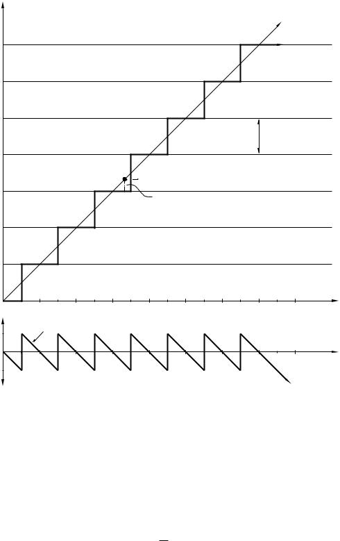
As an example, consider the situation shown in Fig. 14.2, where an input range is represented as a 3-bit code. In essence the process of quantizing a signal is the comparision of the analog value with a fixed number of levels – eight in this case. The nearest level is then taken as expressing the original in its digital equivalent. Thus in Fig. 14.2 an input voltage of 0.4285 of full scale is 0.0536 above quantum level 3. Its quantized value will then be taken as level 3 and coded as 011b in our 3-bit system.
The residual error of −0.0536 will remain as quantizing noise, and can never be eradicated (see Fig. 14.3(d)). The distribution of quantization error is given at the bottom of Fig. 14.2, and is a ected only by the number
14. Take the Rough with the Smooth 393
1 Quantized scale |
|
|
|
|
|
|
|
|
|
in |
|
|
|||
|
Fraction of full scale |
|
|
|
|
|
|
signal |
|
|
|||||
|
|
|
|
|
|
|
|
|
|
||||||
|
|
|
|
|
|
|
|
|
|
|
Analog |
|
|
|
|
7/8 |
|
|
|
|
|
|
|
|
|
|
|
|
|
111 |
|
|
|
|
|
|
|
|
|
|
|
|
|
|
|
||
|
|
|
|
|
|
|
|
|
|
Quantized signal out |
|||||
|
|
|
|
|
|
|
|
|
|
|
|||||
6/7 |
|
|
|
|
|
|
|
|
|
|
|
|
|
|
110 |
|
|
|
|
|
|
|
|
|
|
|
|
|
|
|
|
5/8 |
|
|
|
|
|
|
|
|
|
|
|
|
|
|
101 |
|
|
|
|
|
|
|
|
|
|
|
|
|
|
|
|
|
|
|
|
|
|
|
|
|
|
|
Quantum level L |
||||
4/8 |
|
|
|
|
|
|
|
|
|
|
|
|
|
|
100 |
|
|
|
|
|
|
|
|
|
|
|
|
|
|
|
|
|
|
|
|
|
0.4285 |
|
011 |
|
|
|
|
|
|
011 |
|
3/8 |
|
|
|
|
|
|
|
|
|
|
|
|
|
|
|
|
|
|
|
|
|
|
|
Quantization error |
|
|
|
|
|
|
|
|
|
|
|
|
|
|
|
|
|
|
|
|
|
|
|
2/8 |
|
|
|
|
|
|
|
|
|
|
|
|
|
|
010 |
|
|
|
|
|
|
|
|
|
|
|
|
|
|
|
|
1/8 |
|
|
|
|
|
|
|
|
|
|
|
|
|
|
001 |
|
|
|
|
|
|
|
|
|
|
|
|
|
|
|
|
|
|
|
|
|
|
|
|
|
|
|
|
|
|
|
000 |
0 |
1/16 |
1/8 |
3/16 |
2/8 |
5/16 |
3/8 |
7/16 |
4/8 |
9/16 5/8 11/16 6/8 |
13/16 |
7/8 15/16 |
1 |
Analog scale |
||
|
|||||||||||||||
Error |
|
|
+L/2 |
f(x ) = -(L/X)x +L/2 |
|
|
|
|
0 |
X |
X |
-L/2 |
|
|
Fig. 14.2 The quantizing process.
of levels. This can simply be calculated by evaluating the average of the error function squared. The square root of this is then the root mean square (rms) of the noise.
F(x) = −XL x + L2
The mean square is:
1 |
X |
|
1 |
X |
|
L2 |
L2 |
L2 |
dx |
||
|
0 |
F(x)2 dx = |
|
|
0 |
|
x2 − |
X x + |
|
||
X |
X |
X2 |
4 |
||||||||

394 The Quintessential PIC Microcontroller
|
|
|
|
1 |
|
|
L |
2 |
|
L |
2 |
|
2 |
|
X |
2 |
|||
|
|
|
|
|
|
|
|
|
|
||||||||||
= |
|
|
|
|
|
|
|
x3 − |
|
x2 |
+ L4 x |
|
= 12L |
||||||
|
X |
3 |
|
|
|
2 |
2 |
|
|
||||||||||
|
|
|
X |
|
|
X |
|
|
0 |
|
|||||||||
|
|
|
|
|
|
|
|
|
|
|
|
|
|
|
|
|
|
|
|
|
|
|
|
|
|
|
|
|
|
|
|
|
|
|
|
|
|
|
|
|
L |
|
L |
|
|
|
|
|
|
|
|
|
|
|
|||||
Thus the rms noise value of √ |
|
|
= |
2√ |
|
|
, where L is the quantum level. |
||||||||||||
12 |
3 |
||||||||||||||||||
A fundamental measure of a system’s merit is the signal to noise ratio. Taking the signal to be a sinusoidal wave of peak to peak amplitude 2nL
|
|
|
|
|
|
|
|
|
|
|
|
|
|
n |
|
|
|
|
(see Fig. 14.3), we have an rms signal of |
2 2L |
|
, that is |
peak |
. Thus for a |
|||||||||||||
|
||||||||||||||||||
|
|
|
|
|
|
|
|
|
|
|
|
|
|
√2 |
|
√2 |
||
binary system with n binary bits, we have a signal to noise ratio of: |
||||||||||||||||||
|
|
n |
|
|
2n√ |
|
|
|
|
|
|
|
|
|
|
|
||
|
|
2√L |
|
|
|
|
|
|
|
|
|
|
|
|
|
|||
|
|
12 |
|
|
|
|
|
|
|
|
||||||||
|
2L2 |
|
|
|
|
|
|
1.22 |
|
2n |
|
|
|
|
|
|||
|
|
|
|
|
|
|
|
|
|
|
|
|||||||
|
|
2√2 = |
|
|
|
|
|
|
||||||||||
|
|
√ |
|
= |
|
× |
|
|
|
|
|
|
||||||
|
12 |
|
|
|
|
|
|
|
||||||||||
In decibels we have:
S/N = 20 log 1.22 × 2n = 6.02n + 1.77 dB
The dynamic range of a quantized system is given by the ratio of its full scale (2nL) to its resolution, L. This is just 2n, or in dB, 20 log 2n = 20n log 2 = 6.02n. The percentage resolution given in Table 14.1 is of course just another way of expressing the same thing.
|
Table 14.1: Quantization parameters. |
|
||
Binary bits |
Quantum levels |
% resolution |
Resolution |
S/N ratio (dB) |
n |
(2n) |
|
Dynamic range |
|
4 |
16 |
16.25 |
24.1 dB |
26.9 dB |
8 |
256 |
0.391 |
48.2 dB |
49.9 dB |
10 |
1024 |
0.097 |
60.2 dB |
61.9 dB |
12 |
4096 |
0.024 |
72.2 dB |
74.0 dB |
16 |
65,536 |
0.0015 |
96.3 dB |
98.1 dB |
20 |
1,048,576 |
0.00009 |
120.4 dB |
122.2 dB |
The exponential nature of these quality parameters with respect to the number of binary-word bits is clearly seen in Table 14.1. However, the implementation complexity and thus price also follows this relationship. For example, a 20-bit conversion of 1 V full scale would have to deal with quantum levels less than 1 µV apart. Pulse-code modulated telephonic links use eight bits, but the quantum levels are unequally spaced, being closer at the lower amplitude levels. This reduces quantization hiss where conversations are held in hushed tones! Linear 8-bit conversions are suitable for most general purposes, having a resolution of better than ±14 %. Actually video looks quite acceptable at a 4-bit resolution, and music can just be heard using a single bit – i.e. positive or negative!!

14. Take the Rough with the Smooth 395
S/N ratios presented in Table 14.1 are theoretical upper limits, as errors in the electronic circuitry converting between representations and aliasing (discussed below) will add distortion to the transformation.
The analog world treats time as a continuum, whereas digital systems sample signals at discrete intervals. Shannon’s sampling theorem1 states that provided this interval does not exceed half that of the highest signal frequency, then no information is lost. The reason for this theoretical twice highest frequency sampling limit, called the Nyquist rate, can be seen by examining the spectrum of a train of amplitude modulated pulses. Ideal impulses (pulses with zero width and unit area) are characterized in the frequency domain as a series of equal-amplitude harmonics at the repetition rate, extending to infinity. Real pulses have a similar spectrum but the harmonic amplitudes fall with increasing frequency.
If we modulate this pulse train by a baseband signal A sin ωf t, then in the frequency domain this is equivalent to multiplying the harmonic spectrum (the pulse) by A sin ωf t, giving sum and di erent components thus:
A sin ωf t × B sin ωht = AB2 (sin(ωh + ωf )t + sin(ωh − ωf )t)
More complex baseband signals can be considered to be a bandlimited (fm) collection of individual sinusoids, and on the basis of this analysis each pulse harmonic will sport an upper (sum) and lower (difference) sideband. We can see from the geometry of Fig. 14.3(b) that the harmonics (multiples of the sampling rate) must be spaced at least 2×fm apart, if the sidebands are not to overlap.
A low-pass filter can be used, as shown in Fig. 14.3(d), to recover the baseband from the pulse train. Realizable filters will pass some of the harmonic bands, albeit in an attenuated form. A close examination of the frequency domain of Fig. 14.3(d) shows a vestige of the first lower sideband appearing in the pass band. However, most of the distortion in the reconstituted analog signal is due to the quantizing error resulting from the crude 3-bit digitization. Such a system will have a S/N ratio of around 20 dB.
In order to reduce the demands of the recovery filter, a sampling frequency somewhat above the Nyquist limit is normally used. This introduces a guard band between sidebands. For example the pulse code telephone network has an analog input bandlimited to 3.4 kHz, but is sampled at 8 kHz. Similarly the audio compact disk uses a sampling rate of 44.1 kHz, for an upper music frequency of 20 kHz.
A more graphic illustration of the e ects of sampling at below the Nyquist rate is shown in Fig. 14.4. Here the sampling rate is only 0.75 of the baseband frequency. When the samples are reconstituted by filtering,
1Shannon, C.E.; Communication in the Presence of Noise, Proc. IRE, vol. 37, Jan. 1949, pp. 10–21.

 etc
etc etc
etc14. Take the Rough with the Smooth 397
(a) Sampling below the Nyquist rate
(b) Resulting filtered signal
Fig. 14.4 Illustrating aliasing.
n
Vin Vref ki × 2−i i=1
where ki is the ith binary coe cient having a Boolean value of 0 or 1 and Vin ≤ Vref where Vref is a fixed analog reference voltage. Thus Vin is
expressed as a binary fraction of Vref and the Boolean coe cients k−1 are the required binary digits.
To see how we might implement this in practice, consider the following successive approximation mechanical analogy. Suppose we have an unknown weight W (analogous to Vin), a balance scale (compare to an analog comparator) and a set of precision known weights 1, 2, 4 and 8 gm (analogous to an Vref of 16 gm). A systemic technique based on the task list might be:
1.Place the 8 g weight on the pan. IF too heavy THEN remove (k1 = 0) ELSE leave (k1 = 1).
2.Place the 4 g weight on the pan. IF too heavy THEN remove (k2 = 0) ELSE leave (k2 = 1).
3.Place the 2 g weight on the pan. IF too heavy THEN remove (k3 = 0) ELSE leave (k3 = 1).
4.Place the 1 g weight on the pan. IF too heavy THEN remove (k4 = 0) ELSE leave (k4 = 1).
will yield the nearest lower value as the sum of the weights left on the pan. For example if W were 6.2 g then we would have a weight assemblage of 4 + 2 g or 0110b for a 4-bit system.
The electronic equivalent to this successive approximation technique uses a network of precision resistors or capacitors configured to allow


14. Take the Rough with the Smooth 399
To get to within 0.2% of the final voltage; that is 0.5 of an 8-bit quantum level error, takes approximately 7 × τ. Taken with the 5 µs settling time, the minimum sample time before starting a conversion is around 12 µs. This can be lowered a little by reducing the source resistance. This resistance should not exceed 10 kΩ as pin leakage IL = ±1 µA will give a voltage o set approaching the quantum voltage step. Once charged, the sampling switches disconnect the input pin from the network to hold the voltage constant, so that voltage changes during the conversion period do not a ect the outcome. Thus in a multi-channel ADC module, the channel selection can be changed at this time.
During the sample (S) period, the top capacitor electrodes are held to 0 V and bottom electrodes are charged to Vin. The change-over to the hold (H) position grounds the bottom electrodes and allows the top electrodes to float. The voltage across a capacitor can only change if charge is transferred across electrodes, ∆Q = C∆V. Thus the change in voltage ∆V = −Vin at the bottom electrodes is matched at the top floating electrodes, which now become 0 − Vin, as charge cannot flow in or out of the floating top electrodes. Thus at the start of the conversion process the inverting input of the analog comparator is −Vin.
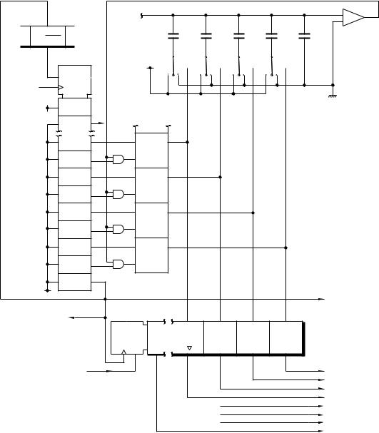
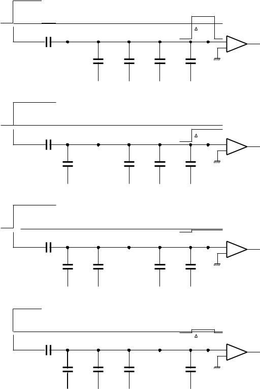
The successive approximation network at the heart of the A/D converter is shown in a simplified form in Fig. 14.6. The step-by-step process is sequenced by a shift register (SRG, see Fig. 2.20 on page 36) when the programmer sets the GO/DONE bit3 in the ADCON0 register (A/D CONtrol 0).4 As the Control shift register is clocked, the single 1 moves down to activate each step in the sequence:
Hold  bit 7
bit 7  bit 6
bit 6  bit 5
bit 5  bit 4
bit 4  bit 3
bit 3  bit 2
bit 2  bit 1
bit 1  bit 0
bit 0 
 Ready
Ready  Sample
The capacitor network is switched to Hold and each capacitor, beginning
with the largest value, is switched to Vref in turn. The outcome of the comparator then determines the state of the corresponding bit in the Succes-
sive Approximation Register (SAR). The process is detailed in Fig. 14.7. After eight set-try-reset actions, the outcome in the SAR is transferred to the Analog to Digital RESult (ADRES) register in File 0Ah. The GO/DONE flag is now cleared to indicate the End Of Conversion and the ADIF flag set. Finally, the analog input is again switched back into the capacitor network (Sample).
The total conversion time is approximately ten times the clocking rate tAD of the sequencer shift register. The minimum clocking period is 1.6 µs (≈ 600 kHz) for all but the older 2 µs PIC16C71/711 devices. There is no specified lower clocking frequency, but as charge slowly leaks away from the network capacitors, a tAD of more than nominally 20 µs (50 kHz)
3GO/DONE can also be set by the CCP2 Comparison special event, see page 375.
4The ADCON0/ADCON1/ADRES registers are at File 1Fh/File 9Fh/File 1Eh respectively in all PIC16C7XX devices except the PIC16C71/710/711, where the corresponding locations are File 08h/File 88h/File 09h.
400 The Quintessential PIC Microcontroller
|
|
|
|
|
|
|
|
|
|
|
+ |
|
|
|
File 08/1Fh |
|
8 |
|
4 |
2 |
1 |
1 |
- |
|
|
R |
|
2 |
|
|
|
|
|
|||||
GO/DONE |
ADCON0 |
|
|
|
|
|
|
|
|
|
||
|
|
|
|
|
|
|
|
|
|
|
||
|
|
SRG10 |
Vref |
D3 |
|
D2 |
D1 |
D0 |
|
|
|
|
|
|
|
|
|
|
|
|
0 V |
|
|
||
|
|
R1 |
|
|
|
|
|
|
|
|
|
|
A/D Clock |
|
-> |
|
|
|
|
|
|
|
|
|
|
|
|
|
|
Successive |
|
|
|
|
|
|
|
|
’1’ |
|
1D |
Approximation |
|
|
|
|
|
|
|
||
|
|
|
Hold |
Register |
|
|
|
|
|
|
|
|
|
|
|
|
|
|
|
|
|
|
|
|
|
|
|
|
|
S |
|
|
|
|
|
|
|
|
|
|
|
|
8 |
|
|
|
|
|
|
|
|
|
|
|
|
R |
|
|
|
|
|
|
|
|
register |
|
|
|
S |
|
|
|
|
|
|
|
|
|
|
|
4 |
|
|
|
|
|
|
|
|
|
|
|
|
R |
|
|
|
|
|
|
|
|
|
|
|
|
|
|
|
|
|
|
|
|
|
|
Shift |
|
|
|
S |
|
|
|
|
|
|
|
|
|
|
|
2 |
|
|
|
|
|
|
|
|
|
|
|
|
R |
|
|
|
|
|
|
|
|
|
|
|
|
|
|
|
|
|
|
|
|
|
|
|
|
|
|
S |
|
|
|
|
|
|
|
|
|
|
|
|
1 |
|
|
|
|
|
|
|
|
|
|
|
|
R |
|
|
|
|
|
|
|
|
|
|
|
|
SAR |
|
|
|
|
|
Conversion |
Complete |
|
’0’ |
|
|
|
|
|
|
|
|
|
|||
|
|
|
|
|
|
|
|
|
|
Sets |
ADIF |
|
|
|
|
|
|
|
|
|
|
|
|
||
|
|
|
A/D |
Result register |
|
|
|
and GO/DONE |
||||
Sample |
|
|
|
File 09/1Eh |
|
|
||||||
|
|
|
|
|
|
|
|
|
|
|||
|
|
|
|
7 |
|
2D |
3 |
2 |
1 |
0 |
|
|
|
|
|
|
|
|
|
|
|
|
ADRES |
|
|
|
|
|
C2 |
E1 |
|
1 |
|
|
|
|
|
|
Read |
Result |
Register |
|
|
|
|
|
|
|
|
|
|
|
|
|
|
|
|
|
|
|
|
MCU to |
Internal bus Data |
|
Fig. 14.6 Simplified view of the A/D converter.
should be avoided. From Fig. 14.8 we see that the ADC clock can be derived from one of four sources using the ADCS1:0 (A/D Clock Select) bits in the ADCON0 SPR. The first three of these are fractions of the MCU clock rate and the fourth is a stand-alone CR oscillator with a nominal tAD of 4 µs.
One of the first tasks a programmer must do is to determine the clocking rate by setting the ADCS1:0 bits appropriately. Table 14.2 shows suggested settings for four typical PIC crystal frequencies. If A/D conversion time is critical then the PIC crystal may be chosen to give the fastest con-

14. Take the Rough with the Smooth 401
Table 14.2: ADC clocking frequency versus device crystal frequency.
ADC clock source tAD |
|
PIC crystal frequency |
|
|||
|
ADSC1:0 |
20 MHz |
8 MHz |
4 MHz |
1 MHz |
100 kHz |
|
|
|
|
|
|
|
fosc/2 |
00 |
— |
— |
— |
2 µs |
20 µs |
fosc/8 |
01 |
— |
— |
2 µs |
8 µs |
— |
fosc/32 |
10 |
1.6 µs |
4 µs |
8 µs |
— |
— |
CR |
11 |
2–6 µs |
2–6 µs |
2–6 µs |
2–6 µs |
2–6 µs |
version time. For example, a 5 MHz crystal with ADCS1:0 = 01 gives a tAD of 1.6 µs.
The internal ADC module CR clock is typically used where the main crystal is below 1 MHz. This separate clock source also allows a conversion to be completed when the PIC is in its Sleep mode, as the main processor oscillator is switched o in this situation. In this case the end of conversion interrupt can be used to awaken the MCU. This gives a relatively quiet environment during the conversion and for this reason is often used even where the processor crystal is above 1 MHz – see Program 14.4.
For lowest current consumption, especially during the Sleep mode, the ADC module should be switched o when not in use by clearing the ADON bit in ADCON0. ADON is cleared on Reset, so needs to be set when the module is to be activated.
The conversion process is illustrated in Fig. 14.7. As we have seen in Fig. 14.5, at the end of the sample period the top plates of the capacitor array are at −Vin and the bottom plates are disconnected but at zero potential. As an example let us assume that Vin is 0.4285Vref.
1.The process begins by switching in Vref into the lower plate of the largest capacitor as controlled by the SAR8 latch in Fig. 14.6. This causes an injection of charge ∆Q = CtotalVref, which is identical across both the 8-unit capacitor C1 and the rest of the capacitors which also have a parallel value of 8 units in Fig. 14.7. Thus the voltage
at node N rises by Vref/2 to −0.485 + 0.5 = +0.07125Vref. In general ∆VN = Vref Ck/Ctotal. The comparator output is now logic 0 and the SAQ8 latch is consequently cleared, reversing the Vref/2 step.
2.SAQ4 switches Vref into the next highest capacitor giving a Vref/4 step at N (124 ). The resulting voltage of −0.485 + 0.25 = −0.178Vref giving a comparator output of logic 1 and SAR4 remains set with the node voltage staying at −0.1785Vref.
3.SAQ2 switches Vref into the second lowest capacitor giving a Vref/8 step at N (162 ). The resulting voltage of −0.1785+0.125 = −0.0535Vref giving a comparator output of logic 1 and SAR2 remains set with the node voltage staying at −0.0535Vref.

14. Take the Rough with the Smooth 403
4.SAQ1 switches Vref into the lowest capacitor giving a Vref/16 step at N (161 ). The resulting voltage of −0.0535+0.0625 = +0.009Vref giving a comparator output of logic 0 and SAR1 is cleared and the Vref/16 step is reversed.
The state of the SAR of 0110b or 0.375Vref represents the best 4-bit fit to Vin = 0.4285Vref. The residue 0.0535Vref is the quantizing error. Most
MCUs use an 8-bit capacitor array. In principle the technique can readily be extended to higher resolutions, but in practice the di culty in matching ever greater capacitors and internal logic noise means the majority of processors use 8-bit resolution. However, a few MCU devices5 do have 10 or 12-bit converters. External successive-approximation devices with 12 or more bits resolution, usually using a resistor ladder network, are readily available, but are relatively expensive.
Matching of the array capacitors, o sets and resistance of internal switches, leakage currents and analog comparator non-linearities all contribute to errors in the conversion process. It is beyond the scope of this text to analyze the various measures of error but the device data sheet lists absolute error, defined as the sum of all component error measures, as better than ±1 LSB. This guarantees that the transfer is monotonic; that is the binary code will never move in the reverse direction for any
change ∆Vin of input voltage. This error figure is for Vref = VDD; if Vref is lower than VDD then accuracy deteriorates, although values down to 3 V
will give acceptable results in most cases. Accuracy can be improved, especially when the internal CR oscillator is used, if the conversion is done while the PIC is in its Sleep mode.
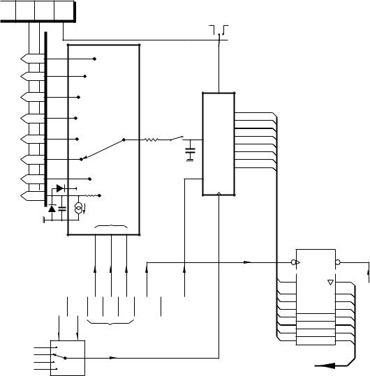
The standard PIC ADC module has eight input channels with any one selected for conversion according to the 3-bit Channel Select code CHS2:0 in the ADCON0 register, as shown in Fig. 14.8. 28-pin footprint PICs, such as the PIC16C73, can only access the bottom five channels. The PIC16C71 line of 18-pin footprint6 and 12C67X devices have an earlier 4-channel module with CHS2 missing. The PIC16C774 uses ADCON0[1] as CHS3.
The input analog channels AN4:0 are shared with the Port A digital inputs RA4:0 and AN7:5 with Port E RE2:0 in 40-pin devices. AN3 is special in that it can be used as the reference voltage input if configured accordingly by PCFG0 = 1 (Port ConFiGuration) bit in the ADCON1 register. Like all port configuration registers it is normally set up only once at the beginning of the program and it is therefore located in the less convenient Bank 1 Data memory. Any such low-noise external Vref should be in the range 3 V → VDD + 0.3 V – see Fig. 14.17. For best accuracy it should be as high as possible; a value of 5.12 V will give a 20 mV per bit resolution.
5For example the PIC16F87X devices have a 10-bit ADC and the PIC16C77X have a 12-bit ADC with internal precision positive and negative reference voltages.
6The PIC16C71/710/711/715.

14. Take the Rough with the Smooth 405
Table 14.3: Configuring the ADC port pins in the PIC16C73/74 devices.
PCFG2:0 |
AN7 |
AN6 |
AN5 |
AN4 |
AN3 |
AN2 |
AN1 |
AN0 |
|
RE2 |
RE1 |
RE0 |
RA5 |
RA3 |
RA2 |
RA1 |
RA0 |
|
|
|
|
|
|
|
|
|
000 |
A |
A |
A |
A |
A |
A |
A |
A |
001 |
A |
A |
A |
A |
Vref |
A |
A |
A |
010 |
D |
D |
D |
A |
A |
A |
A |
A |
011 |
D |
D |
D |
A |
Vref |
A |
A |
A |
100 |
D |
D |
D |
D |
A |
D |
A |
A |
101 |
D |
D |
D |
D |
Vref |
D |
A |
A |
110 |
D |
D |
D |
D |
D |
D |
D |
D |
111 |
D |
D |
D |
D |
D |
D |
D |
D |
page 273) into its linear range and the resulting large current could cause irreversible damage.
Other PIC devices with an ADC module may have di erent settings and numbers of PCFG bits. For example the 8-pin footprint PIC12C67X devices with a 4-channel ADC module can configure individual pins as analog or digital to best use scarce resources. The PIC16C71X line has only the two PCFG bits whilst the PIC16C774 has four.
Vin to A/D converter |
|
|
|
|
+VDD |
|
|
||
|
|
module |
|
|
|
|
|
|
|
|
|
|
|
TRIS |
buffer |
|
I/O |
pin |
|
Data store |
bus |
|
|
|
|
|
|||
1D |
|
|
|
|
|
|
|||
|
|
|
|
|
|
|
|
|
|
Write |
to |
Port |
C1 |
|
|
|
|
|
|
|
|
|
|
|
|
|
|
|
|
|
|
|
Data |
flipflop |
|
|
Overvoltage |
|
|
|
|
|
|
|
|
|
protection |
|
|
|
|
|
1D |
|
|
|
|
|
|
Write |
to |
TRIS |
C1 |
Analog |
input |
|
|
|
|
|
|
|
|
mode |
|
|
|
||
|
|
|
|
|
|
|
|
||
|
|
|
|
|
|
* |
Digital |
|
|
|
|
|
TRIS |
flipflop |
|
input |
buffer |
|
|
|
|
|
|
|
|
||||
To input |
*Port E |
|
|
||
latch |
|
|
|
|
|
Fig. 14.9 Configuring the analog inputs for Port A and Port E.
We can see from Fig. 14.9 that an I/O pin configured as an analog input from ADCON1 simply disables the digital input bu er (compare with Fig. 11.2 on page 273). No other circuitry is a ected. From this we can make the following deductions.

406 The Quintessential PIC Microcontroller
•A port pin configured as analog will read as logic 0 due to the disabled digital input bu er.
•The TRIS bu er is not a ected and thus the appropriate TRIS bits should be 1; that is the direction of the port pins configured as analog
should be set to input to prevent contention between the nalog Vin and the digital state of the Data flip flop.
•The ADC can read an analog voltage at the pin even if that pin has not been configured as analog. However, the still active digital input bu er may consume an excessive current outside of the device’s specification.
Using Fig. 14.8 as the programmer’s model we can now deduce the hardware-software interaction in order to action a conversion. Assuming first that interrupts are not being used, the following steps can be identified:
1.Configure ADC module.
•Set up port pins as analog/voltage reference (ADCON1).
•Select ADC conversion clock source (ADCON0).
•Select ADC input channel (ADCON0).
•Turn on ADC module (ADCON0).
2.Wait for the required acquisition time, typically 12 µs.
3.Start conversion by setting the GO/DONE bit.
4.Wait for ADC conversion to complete by polling the GO/DONE bit for low.
5.Read the ADRES register.
6.For next conversion go to step 1 or step 2 as required.
As an example, consider that we wish to read the channel n analog voltage (RAn) of a PIC16C74 and output the equivalent digital value at
Port B. The main crystal is 20 MHz and VDD is to be used as Vref.
The listing of Program 14.1 assumes that the ADC module has been initialized at reset with startup code of the form:
bsf |
STATUS,RP0 |
; Bank |
1 |
|
|
clrf |
ADCON1 |
; All port inputs are analog |
|||
bcf |
STATUS,RP0 |
; |
Back |
to Bank |
0 |
movlw |
b’10000001’ |
; |
AD clock/32, |
Ch0, no convert, ADON |
|
movwf |
ADCON0 |
|
|
|
|
|
|
|
|
|
|
which sets up the pin configuration according to the PCFGn settings of Table 14.3 to enable all eight ADC channels. The ADCON0 is initialized to 10 000 001b to set the module clock source as the crystal frequency/32;
i.e. 2032 = 625 kHz (giving a conversion time of ≈ 12 +15µs), channel zero
and the module is turned on. With an initial zero value of GO/DONE no conversion is actioned. The initial channel value is irrelevant.
With the module initialized, the subroutine listed in Program 14.1 simply copies the contents of W, truncated to three bits for robustness, into a temporary location TEMP. There it is logic shifted left three places to align the channel number with the CHSn bits in the ADCON0 register.


410 The Quintessential PIC Microcontroller
bsf |
STATUS,RP0 |
; |
Bank 1 |
clrf |
ADCON1 |
; |
All port inputs are analog |
bsf |
PIE1,ADIE |
; |
Enable ADC local interrupt (not PIC16C71) |
bcf |
STATUS,RP0 |
; |
Back to Bank 0 |
movlw |
b’10000001’ ; |
AD clock /32, Ch0, no convert, ADON |
|
movwf |
ADCON0 |
|
|
bcf |
PIR1,ADIF |
; |
ADCON0,ADIF for PIC16C71X |
bsf |
INTCON,PEIE ; |
INTCON,ADIE for PIC16C71X |
|
bsf |
INTCON,GIE |
; |
Enable interrupt subsystem |
|
|
|
|
The interrupt-driven version of our subroutine shown in Program 14.2 is virtually identical to Program 14.1 except that the polling loop at the exit point is eliminated and, of course, no value is returned. However, the 12 µs delay before commencing the process is still needed.
The ISR shown in Program 14.3 is entered when an interrupt (from any source) is generated. For simplicity we assume that there are no other sources of interrupt except from the ADC module. If this is the case, technically the check of the ADIF flag is redundant, although a spurious interrupt can never be ruled out. Where there are multiple sources of interrupt, then each flag can be tested in turn as shown on page 179.
In Program 14.3 a datum file register NEW is cleared to show the background program that the datum byte in ADRES has never been read. When the background routine fetches the digitized byte in ADRES it sets the flag byte NEW to a non-zero value. In a more sophisticated system a bu er of several digitized samples can he maintained by the ISR with NEW giving the number of samples in the bu er – see Example 14.1.
Program 14.2 Interrupt-driven subroutine to read channel n.
; ***********************************************************
; * |
FUNCTION: |
Analog/digital |
conversion at channel n |
* |
|||
; * |
RESOURCE: |
Subroutine |
DELAY_12US, byte TEMP |
* |
|||
; |
* |
ENTRY |
: |
Channel number |
in W |
* |
|
; |
* |
EXIT |
: |
Conversion |
initiated |
* |
|
; ***********************************************************
GET_ANALOG |
|
|
andlw |
b’0111’ |
; Isolate address bits |
movwf |
TEMP |
; Channel number |
bcf |
STATUS,C |
; Shift channel number left >>3 |
rlf |
TEMP,f |
|
rlf |
TEMP,f |
|
rlf |
TEMP,w |
; with outcome in W |
bcf |
ADCON0,CHS0 |
; Zero channel bits |
bcf |
ADCON0,CHS1 |
|
bcf |
ADCON0,CHS2 |
|
addwf |
ADCON0,f |
|
call |
DELAY_12US |
; Wait 12us for things to stabilize |
bsf |
ADCON0,GO |
; Start conversion |
return |
|
|
|
|
|


14. Take the Rough with the Smooth 413
various configuration ports may be accessed in the same manner as at assembly level or, as in Program 14.5, the appropriate compiler built-in functions used to set up and manipulate the SPR control and status bits.
For our example we are going to code a 20 MHz PIC16C74 to act as a comparator in the manner of the Example 11.2 on page 291. Here we want to compare the parallel-input 8-bit word N at Port B with the analog input at Channel 1. Outputs at RC2:0 are to represent Analog Lower Than N, Equivalent and Higher Than N respectively. The comparator is to have a hysteresis of ±1 bit. That is, if previous comparisons showed Analog < N then the trigger level is N + 1 for equality. Similarily, on a downward trajectory the trigger level is decreased to N − 1 for equality.
The function compare() of Program 14.5 assumes that initialization code of the form:
#include |
<16c74.h> |
|
#use |
delay(clock=20000000) |
|
#define |
PORT_B |
*(unsigned int *)0x06 |
#define |
PORT_C |
*(unsigned int *)0x07 |
void compare(unsigned int delta); int main()
{
unsigned int hysteresis = 0; set_tris_c(0xF8); setup_adc(ADC_CLOCK_DIV_32); setup_adc_ports(RA0_RA1_RA3_ANALOG); set_adc_channel(1);
delay_us(12);
has already been executed.
The key internal functions used here are:
setup_adc(ADC_CLOCK_DIV_32);
This function configures bits ADCS1:0 in the ADCON0 to select the module’s clock source; here the processor oscillator/32. The script ADC_CLOCK_INTERNAL may be used to select the internal CR oscillator.
setup_adc_ports(RA0_RA1_RA3_ANALOG);
This configures bits PCFG2:0 in ADCON1 to select which port pins are analog, which are digital and if an external Vref is to be used. The script RA0_RA1_RA3_ANALOG indicates that port lines RA3 and RA1:0 are to be analog with an internal Vref with the rest being digital (PCFG2:0 = 100, see Table 14.3. The equivalent script using an external Vref at RA3 is RA0_RA1_ANALOG_RA3_REF. Scripts appropriate to any aprticular device are stored in the corresponding header file, in this case 16c74.h. All devices with an analog module have scripts ALL_ANALOG and NO_ANALOGS.
set_adc_channel(n);
Used to set up the channel number n in ADCON0, bits CHS2:0.

414 The Quintessential PIC Microcontroller
read_adc();
Activates GO/DONE in ADCON0 and returns with the digitized value from
ADRES when GO/DONE goes to 1.
delay_us(n);
Not explicitely an analog module function; this delays by n µs. The #use delay(clock=20000000) declaration is used by this function to give the delay appropriate for the processor clock frequency.
If the channel number remains constant and the compare() function is not called up at intervals less than the 12 µs settling time (the normal situation) then delay_us(12); can be omitted.
Program 14.5 A digital/analog comparator with hysteresis.
void compare(unsigned int delta)
{
unsigned int analog; analog = read_adc();
if(analog > PORT_B + delta) {PORT_C = 0x04; delta = 0xff;} if(analog == PORT_B) {PORT_C = 0x02;}
else {PORT_C = 0x01; delta = 1;} return delta;
}
The function compare() in Program 14.5 expects the value of the hysteresis, which here is either +1 or −1 (FFh). Internally this is called delta. After the ADC module is read, the digitized value analog is compared with the contents of Port B plus delta and the three Port C bits (RC2:0) set to their appropriate state.
At the same time as the comparison is resolved, delta will be updated to reflect the outcome (i.e. +1 if analog < (PORT_B + delta), −1 if analog > (PORT_B + delta)). The value delta is returned by the function to allow the caller function to update its variable hysteresis. Thus to activate the comparator outputs and also update hysteresis at the same time the caller might have a statement such as hysteresis = compare(hysteresis);. An alternative would be to define the variable hysteresis before the main function main() making it global; that is known to all functions. In this situation its value need not be passed by the caller back and forth to any appropriate function.
The declarations #use fast_io(n); (see page 296) have not been used here as the input(pin) and output_bit(pin,value) internal functions have not been used and the ports have been treated as simple memory bytes.
Conversion from a digital quantity to an analog equivalent is somewhat simpler than the converse and not so commonly required. Perhaps
14. Take the Rough with the Smooth 415
for these reasons digital to analog converters (DACs) are not often found as an integral function in most MCU families.
We have already seen that a rather crude way of providing this mapping is to vary the mark:space ratio of a pulse train of constant repetitive duration, as shown in Fig. 13.9 on page 380. Here a small digital number gives a skinny pulse, which when smoothed out by a low-pass filter (which gives the average or d.c. value) translates to a low voltage. Conversely, a large digital number leads to a correspondingly large mark:space ratio, which in turn after smoothing yields a higher voltage.
PWM conversion can be very accurate and is simple to implement. However, extensive filtering is required to remove harmonics of the pulse rate and this makes the conversion slow to respond to changes in the digital input. Normally PWM is used to control heavy loads, such as motors or heaters, where the inertia of these devices inherently provides the smoothing action. Furthermore, the pulsed nature of the signal is ideally suited to power control, activating thyristor firing circuits.
Many commercial DAC devices are available which can be controlled via standard digital I/O ports. Two examples were given in Figs. 12.4 and 12.6 on pages 310 and 314 where the MCU transferred digital data in series. Here we will look at an example where parallel data transfer is used.
The majority of proprietary devices are based on an R-2R ladder network, such as that shown in Fig. 14.12(a). Voltage appearing at any bit switch node emerges at the output node in an attenuated form. As our analysis will show, each move to the left attenuates this voltage bn by 50%, which is the binary weighting relationship:
N+1
V = bn × 2i
i=0
for an N-bit word.
In Fig. 14.6(b) at mode A looking to the left we see a resistance of R (2R//2R) and the voltage is attenuated by two. As we move to the right the process is repeated with each voltage divided by two. Thus, at node B the voltage b0/2 is further divided by two and the next digital node voltage is divided by two giving VB= b0/4 + b1/2. As the network is symmetrical the resistance looking right at any mode is also 2R. This means that as seen from any digital switch, the total resistance is 2R + 2R//2R = 3R. This is important as the characteristics of a transistor switch, such as resistance, are dependent on current and keeping this the same reduces error.
For clarity our analysis has been for three bits. This can be extended by simply moving the leftmost terminating resistor over and inserting the requisite number of sections. This does not a ect the resistance as seen left of the mode, and therefore does not change the conditions of the

 A
A 
 b
b

14. Take the Rough with the Smooth 417
rightmost sections. An inspection of our analysis shows that nowhere does the absolute value of resistance appear. In fact the accuracy of the analysis depends only on the R:2R ratio. While it is relatively easy to fabricate accurate ratioed resistors on a silicon die, this is certainly not the case for absolute values. For this reason R:2R networks are the standard technique used for most integrated circuit DACs.
The Maxim MAX506 is an example of a commercial D/A converter (DAC). This 20-pin footprint device contains four separate DACs sharing a common external Vref. Digital data is presented to the D7:0 pins and one of four latch registers selected with the A1:0 address inputs. Once this is done, the datum byte is loaded into the selected register n and appears at the corresponding output VOUTn.
This output analog voltage ranges from zero (Analog GrouND) for a
digital input of 00h through to Vref for a digital input of FFh.
Where VSS is connected to ground then Vref can be anything between
0 V and VDD (+5 V). However, VSS can be as low as −5 V and in this case Vref can be anywhere in the range ±5 V. If Vref is negative for dual supplies then the output voltage will also be negative. In either case, e ectively
the output can be treated as the product D × Vref where D is the digital input byte scaled to the range 0 – 1 (00 – FFh).
The MAX505 24-pin variant allows for separate reference voltages to be used for each of the four DAC channels. In addition, the MAX505’s DAC latches are isolated from the converter ladder circuits by a further layer of latches all clocked at the same time with a LDAC (Load DAC) control signal. This double bu ering permits the programmer to update all four DACs simultaneously after their individual latches have been set up.
As an example, consider that a MAX506 quad DAC has its Address selected via RA1:0 and RA2 drives the WR input to latch in the addressed data from Port B. A software routine to generate a continuous staircase sawtooth waveform from DACD would look something like:
movlw |
b’0111’ |
; DACD is channel 3, WR = 1 |
movwf |
PORTA |
; To MAX506 WR, A1:0 |
LOOP movwf |
PORTB |
; Datum to MAX506’s D7:0 |
bcf |
PORTA,2 |
; WR = 0; Latch datum in |
bsf |
PORTA,2 |
; WR = 1; by pulsing WR |
addlw |
1 |
; Increment staircase count |
goto |
LOOP |
; and repeat forever |
|
|
|
where we are assuming that Port B and Port A[2:0] have been set up as outputs.
A typical DAC staircase output waveform is shown in the oscillogram in Fig. 14.13. Here a 12 MHz crystal clocked PIC is shown which, with a
 VDD
VDD VSS
VSS DGND
DGND


 Vout(A)
 Vout(B)
 A1
A1 A0
A0 Vout(C)
 Vout(C)
 WR
WR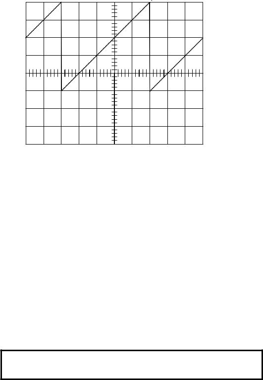
14. Take the Rough with the Smooth 419
1 V/div
TIME BASE 0.1 ms/div
Fig. 14.13 Generating a continuous sawtooth using a MAX506 DAC.
loop cycle count of 6 cycles, gives a sawtooth duration of (256 × 6)/3 ≈ 0.5 ms at 2 µs per step.
Examples
Example 14.1
Augment the interrupt-driven ISR of Program 14.2 to implement a 16deep bu er array of data to allow a limited mismatch between acquisition and reading rates.
Solution
One approach is shown in Fig. 14.14. A block of file registers is set aside by the programmer together with any other variables used by the programmer with a cblock directive of the form:
cblock
ARRAY:16, OVERFLOW:1, BUF_EMPTY:1, ... ; etc. endc
and the File Select Register used as a bu er pointer to the next empty location in the array of samples.
In acquiring data the foreground ISR of Program 14.6 simply pushes the datum from the ADRES into the location pointed to by the FSR using

420 The Quintessential PIC Microcontroller
ARRAY
FSR 
datum
Interrupt
Fig. 14.14 Bu ered data acquisition.
the indirect address mode and then increments this pointer ready for the next event.
The problem with this approach is that if the background program does not pull data out of the bu er quickly enough, decrementing the FSR, the bu er will overflow. As a consequence, if there are variables stored above ARRAY+15 then they will be overwritten. In order to avoid this problem, on overflow no more data should be saved and the state of the OVERFLOW file register set to non zero to show the background software that data has been lost.
Based on this ISR, a background routine to fetch data from the bu er would be something like this:
GET_IT bcf |
INTCON,GIE |
; Disable interrupts |
btfsc |
INTCON,GIE |
; Make sure |
goto |
GET_IT |
; IF not THEN DO again |
clrf |
BUF_EMPTY |
; Zero Buffer-Empty flag |
movf |
FSR,w |
; Check is FSR below ARRAY? |
sublw |
ARRAY |
; ARRAY - FSR |
btfsc |
STATUS,C |
; IF FSR is EQUAL or LESS THAN |
goto |
CONTINUE |
; IF so THEN buffer is empty |
decf |
BUF_EMPTY,f |
; ELSE show buffer is not empty |
movf |
0,w |
; Get datum |
decf |
FSR,f |
; Decrement buffer pointer |
CONTINUEbsf |
INTCON,GIE |
; and re-enable interrupt |

14. Take the Rough with the Smooth 421
Program 14.6 Bu ered interrupt-driven data acquisition.
;**********************************************************
;* FUNCTION: ISR to read the A/D converter at EOC and put *
; * |
FUNCTION: |
in buffer |
if not full |
and update pointer |
* |
|||||
; * |
ENTRY |
: |
On an interrupt. |
FSR |
points to last entry |
* |
||||
; * |
EXIT |
: |
FSR incremented and new datum |
pushed into buf* |
||||||
; |
* |
EXIT |
: |
IF buffer |
is |
full |
OVERFLOW is |
returned as -1 * |
||
; |
* |
EXIT |
: |
ELSE returns |
zero |
|
|
|
* |
|
;**********************************************************
;First save context
A_D_ISR movwf |
_work |
; |
Put |
away W |
swapf |
STATUS,w |
; |
and |
the Status register |
movwf |
_status |
|
|
|
; ************************************************************
|
btfss |
PIR1,ADIF |
; |
Check; has there been a conversion |
|
goto |
ISR_EXIT |
; |
IF not THEN false alarm |
|
incf |
FSR,w |
; |
Move pointer up to the next location |
|
sublw |
ARRAY+d’16’; |
FSR - (ARRAY+16) Outside the buffer? |
|
|
btfsc |
STATUS,C |
; |
IF yes |
|
goto |
FULL |
; |
THEN can’t update |
|
clrf |
OVERFLOW |
; |
Zero teh overflow flag |
|
incf |
FSR,f |
; |
ELSE update pointer |
|
movf |
ADRES,w |
; |
and get digitized byte |
|
movwf |
INDF |
; |
and put in buffer |
|
goto |
ISR_EXIT |
; |
and exit gracefully |
FULL |
movlw |
-1 |
; |
Show the world that buffer |
|
movwf |
OVERFLOW |
; |
has overflowed |
; ************************************************************
ISR_EXIT swapf |
_status,w |
; Untwist |
the original Status reg |
||
movwf |
STATUS |
|
|
|
|
swapf |
_work,f |
; Get |
the |
original W reg back |
|
swapf |
_work,w |
; |
leaving |
STATUS unchanged |
|
retfie |
|
; |
and |
return from interrupt |
|
|
|
|
|
|
|
It is essential to avoid any alteration to the FSR during a background bu er fetch, so GIE is zeroed before and enabled after the process to disable interrupts. If the bu er pointer is at the bottom of the array then no update is carried out and the file register EMPTY is left at zero to show that the bu er was empty. Otherwise the datum pointed to is copied to the Working register; the bu er pointer is decremented and EMPTY is set to non zero.


14. Take the Rough with the Smooth 425
Program 14.8 ECG peak picking.
; ***********************************************************
; * |
FUNCTION: |
ISR to |
update the ECG |
parameters |
* |
||
; |
* |
ENTRY |
: |
On a Timer0 interrupt |
|
* |
|
; |
* |
EXIT |
: |
Update |
MAXIMUM and THRESHOLD:THRESHOLD+1 |
* |
|
;***********************************************************
;First save context
ECG_ISR movwf |
_work |
; |
Put |
away W |
swapf |
STATUS,w |
; |
and |
the Status register |
movwf |
_status |
|
|
|
; ************************************************************
|
btfss |
INTCON,T0IF |
; |
Was this a Timer0 interrupt? |
|
goto |
ECG_EXIT |
; |
IF not THEN exit |
|
bcf |
INTCON,T0IF |
; ELSE clear flag |
|
|
movlw |
1 |
; |
Initiate a conversion of |
|
call |
GET_ANALOG |
; |
Channel 1 |
|
movwf |
TEMP |
; |
Save digitized value |
|
subwf |
THRESHOLD,w |
; |
THRESHOLD - ANALOG |
|
btfsc |
STATUS,C |
; |
IF no Borrow THEN |
|
goto |
BELOW |
; |
don’t update MAXIMUM |
|
movf |
TEMP,w |
; |
ELSE get digitized value |
|
movwf |
MAXIMUM |
; |
which is the new MAXIMUM |
|
movwf |
PORTB |
; |
made visible to outside |
|
bsf |
PORTA,5 |
; |
which is signalled |
|
movwf |
THRESHOLD |
; |
Now update double-byte |
|
clrf |
THRESHOLD+1 |
; |
threshold |
|
goto |
ECG_EXIT |
; |
and finish |
; Land here if the input is below the threshold |
||||
BELOW |
bcf |
PORTA,5 |
; |
Signal no update |
; Now reduce the threshold by 0.5 unless it is zero |
||||
|
movf |
THRESHOLD,f |
; |
Is integer threshold zero? |
|
btfsc |
STATUS,Z |
; |
Skip if not |
|
goto |
ECG_EXIT |
; |
IF it is THEN leave alone |
|
movlw |
80h |
; |
0.5 = 10000000b |
|
subwf |
THRESHOLD+1,f ; |
Take away from fraction byte |
|
|
btfss |
STATUS,C |
; |
Skip if no borrow |
|
decf |
THRESHOLD,f |
; |
ELSE decrement integer thres |
; ************************************************************
ECG_EXIT swapf |
_status,w |
; Untwist the original Status reg |
||
movwf |
STATUS |
|
|
|
swapf |
_work,f |
; Get |
the original W reg back |
|
swapf |
_work,w |
; |
leaving STATUS unchanged |
|
retfie |
|
; |
and |
return from interrupt |
|
|
|
|
|
426 The Quintessential PIC Microcontroller
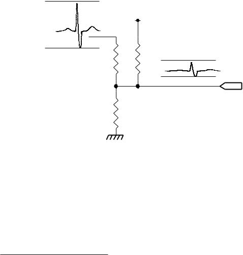
Vref |
THRESHOLD |
|
0V
Fig. 14.16 ECG detection strategy.
2.IF (ANALOG > THRESHOLD)
•MAXIMUM = ANALOG.
•THRESHOLD = ANALOG.
•PORTB = ANALOG.
•RA5 = 1.
3.ELSE
•Reduce THRESHOLD by 0.5.
•RA5 = 0.
In updating THRESHOLD where ANALOG > THRESHOLD the integer byte takes the new value of MAXIMUM whilst the fractional byte is zeroed. Treating this byte pair as a 16-bit word, this e ectively equates the threshold as MAXIMUM × 256 or THRESHOLD = MAXIMUM << 8, where MAXIMUM has been shifted left eight places. We are assuming that THRESHOLD has been zeroed in the background program during the initialization phase.
If the digitized analog sample is less than the threshold trip value then 80h = 10000000b is subtracted from the lower byte at THRESHOLD+1 and if this produces a borrow, then the upper byte at THRESHOLD is decremented. This subtract 12 routine is skipped if the threshold has reached zero thus preventing underflow.
Although not shown, Program 14.8 uses the subroutine GET_ANALOG of Program 14.1 and its associated 12 µs delay subroutine.
Program 14.9 gives the C coded version implementing our task list. The #int_rtcc directive tells the compiler to treat the following function as a Real-Time Counter Clock (Timer 0) ISR. In function ecg_isr(), the variables threshold and maximum are declared static. This means that their value will be retained after the function has exited and will be available next time on entry. The default way of treating C function variables is to hold their value only for the duration of the function. An alternative way of dealing with this problem is to declare such variables outside any function, in which case they will be global and retain their value indefinitely.
threshold is defined as a long int and the CCS compiler will then treat this datum as a 16-bit variable as required. The definition in equating threshold to zero will only initialize it once when the program begins
14. Take the Rough with the Smooth 427
Program 14.9 An implementation of the ECG peak picker in C.
#int_rtcc ecg_isr()
{
unsigned int analog;
static unsigned long int threshold = 0; static unsigned int maximum;
analog = read_adc();
if(analog > threshold>>8) |
|
|
|
{ |
|
|
|
maximum |
= analog; |
/* New maximum value |
*/ |
PORT_B |
= analog; |
/* Show the outside world |
*/ |
threshold = maximum << 8; |
/* New 2-byte threshold |
*/ |
|
output_bit(PIN_A5,1); |
/* Tell outside world |
*/ |
|
} |
|
|
|
else |
|
|
|
{ |
|
|
|
threshold = threshold - 0x0080; /* Reduce by 0.5 |
*/ |
||
output_bit(PIN_A5,0); |
/* Signal no update |
*/ |
|
} |
|
|
|
} |
|
|
|
its run, as the variable is static. Again this is not the normal behavior of the default auto variable.
In equating threshold to the new maximum value, the latter is multiplied by 256 by shifting left eight times – a good compiler will automatically change a N*256 to N<<8. This double-byte form allows for the reduction by half a bit 0080h to give the specified falling trip level.
Both implementations assume that the analog module, ports and interrupt mask bits have been set up at the beginning of the background program as described earlier in the chapter.
Self-assessment questions
14.1 In Example 14.4 the decay of the threshold level was linear. Although this is fairly e ective for situations where the nominal period is known a priori and does not vary greatly, an exponential decay would be better suited where this is not the case. To generate this type of relationship a fixed percentage of the value at each sample point should be subtracted to give the new outcome rather than a constant. Show how you could modify Programs 14.8 and 14.9 to decrement at a rate of approximately 0.4% (≈ 2561 ) on each sample and determine the time constant in terms of the number of samples.

428The Quintessential PIC Microcontroller
14.2A programmer writing an ISR-based handler for an analog module has replaced the retfie instruction in Program 14.2 by return. What e ect will this have?
14.3Real world analog signals are noisy. In practice this means that some form of filtering or smoothing is frequently required. In any circumstance noise coming in from outside should not have any appreciable frequency components above half the sampling rate since such noise will be frequency shifted back into the baseband as shown in Fig. 14.4. Such low-pass filtering must be applied to the signal before the A/D conversion.
Although this external anti-alias filter must by definition be implemented using hardware circuitry (such as a CR network), noise within the passband can be smoothed out using software filtering routines. One simple approach to digital filtering is to take multiple readings and average them to give a composite outcome. For example, 16
readings summed and shifted right four times (÷16) would reduce random noise by a factor of √16 = 4.
Another approach well known to staticians, is to take a moving average; for example, of a stock price over a month interval. An e cient algorithm of this type is a 3-point average:
Array[i] = S4n + Sn2−1 + Sn4−2
where Sn is the nth sample from the analog module.
Show how you could modify the GET_ANALOG subroutine to remember the last samples from the two previous calls and return the smoothed value.
14.4 It has been suggested that as part of the ECG monitor of Example 14.4 that a MAX506 DAC be used to introduce an automatic gain control function preceding the PIC’s analog input. The aim of the AVC is to keep the peak of the analog input between 34 and 78 full scale. How might you go about implementing this subsystem? Hint: Remember that each channel of a MAX506 is the product of its digital input and Vref and that the latter can vary between 0 V and VDD.
14.5How could the time between ECG peaks be measured with a resolution of 10 ms and output at one of the parallel ports as an extension of Example 14.4?
14.6An input analog sinusoid signal, conditioned as shown in Fig. 14.15, is to be full-wave rectified; that is voltages that were originally negative are to have their sign changed. Design a routine to do this assuming that the input voltage is available at ADRES and the processed output is to be presented via Port B to a DAC.