- •Introduction
- •ARM7TDMI Architecture
- •The THUMB Concept
- •THUMB’s Advantages
- •ARM7TDMI Block Diagram
- •ARM7TDMI Core Diagram
- •ARM7TDMI Functional Diagram
- •Key to signal types
- •Processor Operating States
- •Switching State
- •Entering THUMB state
- •Entering ARM state
- •Memory Formats
- •Big endian format
- •Little endian format
- •Instruction Length
- •Data Types
- •Operating Modes
- •Registers
- •The ARM state register set
- •The THUMB state register set
- •The relationship between ARM and THUMB state registers
- •Accessing Hi registers in THUMB state
- •The Program Status Registers
- •The condition code flags
- •The control bits
- •Exceptions
- •Action on entering an exception
- •Action on leaving an exception
- •Exception entry/exit summary
- •Notes
- •Abort
- •Software interrupt
- •Undefined instruction
- •Exception vectors
- •Exception priorities
- •Not all exceptions can occur at once:
- •Interrupt Latencies
- •Reset
- •Instruction Set Summary
- •Format summary
- •Instruction summary
- •The Condition Field
- •Branch and Exchange (BX)
- •Instruction cycle times
- •Assembler syntax
- •Using R15 as an operand
- •Examples
- •Branch and Branch with Link (B, BL)
- •The link bit
- •Instruction cycle times
- •Assembler syntax
- •Examples
- •Data Processing
- •CPSR flags
- •Shifts
- •Instruction specified shift amount
- •Register specified shift amount
- •Immediate operand rotates
- •Writing to R15
- •Using R15 as an operand
- •TEQ, TST, CMP and CMN opcodes
- •Instruction cycle times
- •Assembler syntax
- •where:
- •Examples
- •PSR Transfer (MRS, MSR)
- •Operand restrictions
- •Reserved bits
- •Example
- •Instruction cycle times
- •Assembler syntax
- •Examples
- •Multiply and Multiply-Accumulate (MUL, MLA)
- •If the operands are interpreted as signed
- •If the operands are interpreted as unsigned
- •Operand restrictions
- •CPSR flags
- •Instruction cycle times
- •Assembler syntax
- •Examples
- •Multiply Long and Multiply-Accumulate Long (MULL,MLAL)
- •Operand restrictions
- •CPSR flags
- •Instruction cycle times
- •For signed instructions SMULL, SMLAL:
- •For unsigned instructions UMULL, UMLAL:
- •Assembler syntax
- •where:
- •Examples
- •Single Data Transfer (LDR, STR)
- •Offsets and auto-indexing
- •Shifted register offset
- •Bytes and words
- •Little endian configuration
- •Big endian configuration
- •Restriction on the use of base register
- •Example:
- •Data aborts
- •Instruction cycle times
- •Assembler syntax
- •Examples
- •Halfword and Signed Data Transfer(LDRH/STRH/LDRSB/LDRSH)
- •Offsets and auto-indexing
- •Halfword load and stores
- •Signed byte and halfword loads
- •Endianness and byte/halfword selection
- •Little endian configuration
- •Big endian configuration
- •Data aborts
- •Instruction cycle times
- •Assembler syntax
- •Examples
- •Block Data Transfer (LDM, STM)
- •The register list
- •Addressing modes
- •Address alignment
- •LDM with R15 in transfer list and S bit set (Mode changes)
- •STM with R15 in transfer list and S bit set (User bank transfer)
- •R15 not in list and S bit set (User bank transfer)
- •Use of R15 as the base
- •Inclusion of the base in the register list
- •Data aborts
- •Aborts during STM instructions
- •Aborts during LDM instructions
- •Instruction cycle times
- •Assembler syntax
- •Addressing mode names
- •Examples
- •Single Data Swap (SWP)
- •Bytes and words
- •Data aborts
- •Instruction cycle times
- •Assembler syntax
- •Examples
- •Software Interrupt (SWI)
- •Return from the supervisor
- •Comment field
- •Instruction cycle times
- •Assembler syntax
- •Examples
- •Supervisor code
- •Coprocessor Data Operations (CDP)
- •The coprocessor fields
- •Instruction cycle times
- •Assembler syntax
- •Examples
- •Coprocessor Data Transfers (LDC, STC)
- •The coprocessor fields
- •Addressing modes
- •Address alignment
- •Data aborts
- •Instruction cycle times
- •Assembler syntax
- •Examples
- •Coprocessor Register Transfers (MRC, MCR)
- •The coprocessor fields
- •Transfers to R15
- •Transfers from R15
- •Instruction cycle times
- •Assembler syntax
- •Examples
- •Undefined Instruction
- •Instruction cycle times
- •Assembler syntax
- •Instruction Set Examples
- •Using the conditional instructions
- •Using conditionals for logical OR
- •Absolute value
- •Multiplication by 4, 5 or 6 (run time)
- •Combining discrete and range tests
- •Division and remainder
- •Overflow detection in the ARM7TDMI
- •Pseudo-random binary sequence generator
- •Multiplication by constant using the barrel shifter
- •Multiplication by 2^n (1,2,4,8,16,32..)
- •Multiplication by 2^n+1 (3,5,9,17..)
- •Multiplication by 2^n-1 (3,7,15..)
- •Multiplication by 6
- •Multiply by 10 and add in extra number
- •General recursive method for Rb := Ra*C, C a constant:
- •Loading a word from an unknown alignment
- •Format Summary
- •Opcode Summary
- •Format 1: move shifted register
- •Operation
- •Instruction cycle times
- •Examples
- •Format 2: add/subtract
- •Operation
- •Instruction cycle times
- •Examples
- •Format 3: move/compare/add/subtract immediate
- •Operations
- •Instruction cycle times
- •Examples
- •Format 4: ALU operations
- •Operation
- •Instruction cycle times
- •Examples
- •Format 5: Hi register operations/branch exchange
- •Operation
- •Instruction cycle times
- •The BX instruction
- •Examples
- •Using R15 as an operand
- •Format 6: PC-relative load
- •Operation
- •Instruction cycle times
- •Examples
- •Format 7: load/store with register offset
- •Operation
- •Instruction cycle times
- •Examples
- •Format 8: load/store sign-extended byte/halfword
- •Operation
- •Instruction cycle times
- •Examples
- •Format 9: load/store with immediate offset
- •Operation
- •Instruction cycle times
- •Examples
- •Format 10: load/store halfword
- •Operation
- •Instruction cycle times
- •Examples
- •Format 11: SP-relative load/store
- •Operation
- •Instruction cycle times
- •Examples
- •Format 12: load address
- •Operation
- •Instruction cycle times
- •Examples
- •Format 13: add offset to Stack Pointer
- •Operation
- •Instruction cycle times
- •Examples
- •Format 14: push/pop registers
- •Operation
- •Instruction cycle times
- •Examples
- •Format 15: multiple load/store
- •Operation
- •Instruction cycle times
- •Examples
- •Format 16: conditional branch
- •Operation
- •Instruction cycle times
- •Examples
- •Format 17: software interrupt
- •Operation
- •Instruction cycle times
- •Examples
- •Format 18: unconditional branch
- •Operation
- •Examples
- •Format 19: long branch with link
- •Operation
- •Instruction cycle times
- •Examples
- •Instruction Set Examples
- •Multiplication by a constant using shifts and adds
- •General purpose signed divide
- •Thumb code
- •ARM code
- •Division by a constant
- •Explanation of divide-by-constant ARM code
- •ARM code
- •THUMB code
- •Overview
- •Cycle Types
- •Address Timing
- •Data Transfer Size
- •Instruction Fetch
- •Memory Management
- •Locked Operations
- •Stretching Access Times
- •The ARM Data Bus
- •The External Data Bus
- •The unidirectional data bus
- •The bidirectional data bus
- •Example system: The ARM7TDMI Testchip
- •Overview
- •Interface Signals
- •Coprocessor present/absent
- •Busy-waiting
- •Pipeline following
- •Data transfer cycles
- •Register Transfer Cycle
- •Privileged Instructions
- •Idempotency
- •Undefined Instructions
- •Debug Interface
- •Overview
- •Debug Systems
- •Debug Interface Signals
- •Entry into debug state
- •Entry into debug state on breakpoint
- •Entry into debug state on watchpoint
- •Entry into debug state on debug-request
- •Action of ARM7TDMI in debug state
- •Scan Chains and JTAG Interface
- •Scan limitations
- •Scan chain 0
- •Scan chain 1
- •Scan Chain 2
- •The JTAG state machine
- •Reset
- •Pullup Resistors
- •Instruction Register
- •Public Instructions
- •EXTEST (0000)
- •SCAN_N (0010)
- •INTEST (1100)
- •IDCODE (1110)
- •BYPASS (1111)
- •CLAMP (0101)
- •HIGHZ (0111)
- •CLAMPZ (1001)
- •SAMPLE/PRELOAD (0011)
- •RESTART (0100)
- •Test Data Registers
- •Bypass register
- •ARM7TDMI device identification (ID) code register
- •Operating mode:
- •Instruction register
- •Scan chain select register
- •Scan chains 0,1 and 2
- •Scan chain 0 and 1
- •Scan chain 0
- •Scan chain 1
- •Scan chain 3
- •ARM7TDMI Core Clocks
- •Clock switch during debug
- •Clock switch during test
- •Determining the Core and System State
- •Determining the core’s state
- •Determining system state
- •Exit from debug state
- •The PC’s Behaviour During Debug
- •Breakpoint
- •Watchpoints
- •Watchpoint with another exception
- •Debug request
- •System speed access
- •Summary of return address calculations
- •Priorities / Exceptions
- •Breakpoint with prefetch abort
- •Interrupts
- •Data aborts
- •Scan Interface Timing
- •Debug Timing
- •Overview
- •The Watchpoint Registers
- •Programming and reading watchpoint registers
- •Using the mask registers
- •The control registers
- •Programming Breakpoints
- •Hardware breakpoints:
- •Software breakpoints:
- •Hardware breakpoints
- •Software breakpoints
- •Setting the breakpoint
- •Clearing the breakpoint
- •Programming Watchpoints
- •The Debug Control Register
- •Debug Status Register
- •Coupling Breakpoints and Watchpoints
- •Example
- •CHAINOUT signal
- •RANGEOUT signal
- •Example
- •Disabling ICEBreaker
- •ICEBreaker Timing
- •Programming Restriction
- •Debug Communications Channel
- •Debug comms channel registers
- •Communications via the comms channel
- •Introduction
- •Branch and Branch with Link
- •THUMB Branch with Link
- •Branch and Exchange (BX)
- •Data Operations
- •Multiply and Multiply Accumulate
- •Load Register
- •Store Register
- •Load Multiple Registers
- •Store Multiple Registers
- •Data Swap
- •Software Interrupt and Exception Entry
- •Coprocessor Data Operation
- •Coprocessor Data Transfer (from memory to coprocessor)
- •Coprocessor Data Transfer (from coprocessor to memory)
- •Coprocessor Register Transfer (Load from coprocessor)
- •Coprocessor Register Transfer (Store to coprocessor)
- •Undefined Instructions and Coprocessor Absent
- •Unexecuted Instructions
- •Instruction Speed Summary
- •Timing Diagrams
Single Data Swap (SWP)
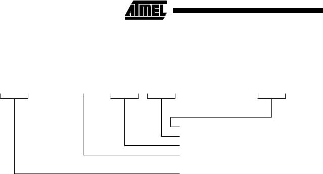
Figure 32. Swap Instruction
31 |
28 |
27 |
23 |
22 |
21 |
20 |
19 |
16 |
15 |
12 |
11 |
8 |
7 |
4 |
3 |
0 |
|
Cond |
|
00010 |
B |
00 |
Rn |
|
|
Rd |
|
0000 |
|
1001 |
|
Rm |
|
|
|
|
|
|
|
|
|
|
|
|
|
|
|
|
|
|
The instruction is only executed if the condition is true. The various conditions are defined in Table 6. The instruction encoding is shown in Figure 32.
The data swap instruction is used to swap a byte or word quantity between a register and external memory. This instruction is implemented as a memory read followed by a memory write which are “locked” together (the processor cannot be interrupted until both operations have completed, and the memory manager is warned to treat them as inseparable). This class of instruction is particularly useful for implementing software semaphores.
The swap address is determined by the contents of the base register (Rn). The processor first reads the contents of the swap address. Then it writes the contents of the source register (Rm) to the swap address, and stores the old memory contents in the destination register (Rd). The same register may be specified as both the source and destination.
The LOCK output goes HIGH for the duration of the read and write operations to signal to the external memory manager that they are locked together, and should be allowed to complete without interruption. This is important in multiprocessor systems where the swap instruction is the only indivisible instruction which may be used to implement semaphores; control of the memory must not be removed from a processor while it is performing a locked operation.
Source register
Destination register
Base register
Byte/Word bit
0 = swap word quantity
1 = swap byte quantity
Condition field
Bytes and words
This instruction class may be used to swap a byte (B=1) or a word (B=0) between an ARM7TDMI register and memory. The SWP instruction is implemented as a LDR followed by a STR and the action of these is as described in the section on single data transfers. In particular, the description of Big and Little Endian configuration applies to the SWP instruction.
Use of R15
Do not use R15 as an operand (Rd, Rn or Rs) in a SWP instruction.
Data aborts
If the address used for the swap is unacceptable to a memory management system, the memory manager can flag the problem by driving ABORT HIGH. This can happen on either the read or the write cycle (or both), and in either case, the Data Abort trap will be taken. It is up to the system software to resolve the cause of the problem, then the instruction can be restarted and the original program continued.
Instruction cycle times
Swap instructions take 1S + 2N +1I incremental cycles to execute, where S,N and I are as defined in Cycle Types.
62 Instruction Set
Instruction Set
Assembler syntax
<SWP>{cond}{B} Rd,Rm,[Rn]
{cond} two-character condition mnemonic. See Table 6.
{B} if B is present then byte transfer, otherwise word transfer
Rd,Rm,Rn are expressions evaluating to valid register numbers
Examples
SWP |
R0,R1,[R2] |
; Load R0 with the word addressed by R2, and |
|
|
; store R1 at R2. |
SWPB |
R2,R3,[R4] |
; Load R2 with the byte addressed by R4, and |
|
|
; store bits 0 to 7 of R3 at R4. |
SWPEQ R0,R0,[R1] |
; Conditionally swap the contents of the |
|
|
|
; word addressed by R1 with R0. |
63