


About this document
This document is the technical reference manual for the ARM PrimeCell Smart Card Interface (SCI).
Intended audience
This document has been written for System-on-Chip (SoC) designers and system architects, and provides a description of components within the SCI architecture.
Using this manual
This document is organized into the following chapters:
Chapter 1 Introduction
Read this chapter for an introduction on the ARM PrimeCell SCI and its features.
Chapter 2 Functional Overview
Read this chapter for a description of the block diagram and functionality of the PrimeCell SCI.
Chapter 3 Programmer’s Model
Read this chapter for a description of the PrimeCell SCI registers and programming details.
Chapter 4 Programmer’s Model for Test
Read this chapter for an description of the logic in the PrimeCell SCI for integration testing.
Appendix A ARM PrimeCell SCI (PL131) Signal Descriptions
Read this chapter for a description of the AMBA APB signals, on-chip signals and signals to pads.
vi |
Copyright © 2001 ARM Limited. All rights reserved. |
ARM DDI 0228A |

Typographical conventions
The following typographical conventions are used in this document:
bold |
Highlights ARM processor signal names, and interface elements |
|
such as menu names. Also used for terms in descriptive lists, |
|
where appropriate. |
italic |
Highlights special terminology, cross-references, and citations. |
monospace |
Denotes text that can be entered at the keyboard, such as |
|
commands, file names and program names, and source code. |
monospace |
Denotes a permitted abbreviation for a command or option. The |
|
underlined text can be entered instead of the full command or |
|
option name. |
monospace italic |
Denotes arguments to commands or functions where the argument |
|
is to be replaced by a specific value. |
monospace bold |
Denotes language keywords when used outside example code. |
ARM DDI 0228A |
Copyright © 2001 ARM Limited. All rights reserved. |
vii |
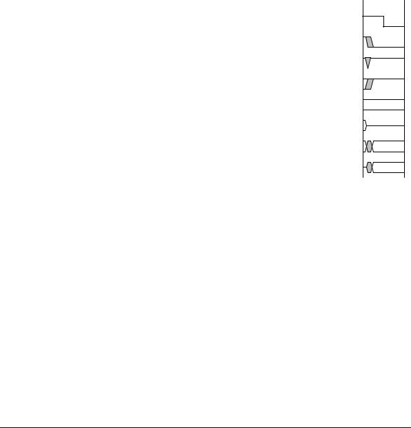
Timing diagram conventions
This manual contains one or more timing diagrams. The following key explains the components used in these diagrams. Any variations are clearly labeled when they occur. Therefore, no additional meaning should be attached unless specifically stated.
Clock
HIGH to LOW
Transient
HIGH/LOW to HIGH
Bus stable
Bus to high impedance
Bus change
High impedance to stable bus
Key to timing diagram conventions
Shaded bus and signal areas are undefined, so the bus or signal can assume any value within the shaded area at that time. The actual level is unimportant and does not affect normal operation.
viii |
Copyright © 2001 ARM Limited. All rights reserved. |
ARM DDI 0228A |