


Programmer’s Model
Note
When you design a systems memory map you must remember that the register has a 4KB-memory footprint.
The 4-bit revision number is implemented by instantiating a component called RevisionAnd four times with its inputs tied off as appropriate, and the output sent to the read multiplexor.
All memory accesses to the peripheral identification registers must be 32-bit, using the LDR and STR instructions.
The four, 8-bit peripheral identification registers are described in the following subsections:
•MMCIPeriphID0 register
•MMCIPeriphID1 register on page 3-19
•MMCIPeriphID2 register on page 3-19
•MMCIPeriphID3 register on page 3-19.
MMCIPeriphID0 register
The MMCIPeriphID0 register is hard coded and the fields within the registers determine the reset value. Table 3-20 shows the bit assignment of the MMCIPeriphID0 register.
|
|
|
Table 3-20 MMCIPeriphID0 register |
|
|
|
|
Bits |
Name |
Type |
Function |
|
|
|
|
31:8 |
- |
- |
Reserved, read undefined, must be written as zeros. |
|
|
|
|
7:0 |
Partnumber0 |
Read |
These bits read back as 0x81. |
|
|
|
|
3-18 |
Copyright © 2000, 2001 ARM Limited. All rights reserved. |
ARM DDI 0205B |

Programmer’s Model
MMCIPeriphID1 register
The MMCIPeriphID1 register is hard coded and the fields within the registers determine the reset value. Table 3-21 shows the bit assignment of the MMCIPeriphID1 register.
|
|
|
Table 3-21 MMCIPeriphID1 register |
|
|
|
|
Bits |
Name |
Type |
Function |
|
|
|
|
31:8 |
- |
- |
Reserved, read undefined, must be written as zeros. |
|
|
|
|
7:4 |
Designer0 |
Read |
These bits read back as 0x1. |
|
|
|
|
3:0 |
Partnumber1 |
Read |
These bits read back as 0x1. |
|
|
|
|
MMCIPeriphID2 register
The MMCIPeriphID2 register is hard coded and the fields within the registers determine the reset value. Table 3-22 shows the bit assignment of the MMCIPeriphID2 register.
|
|
|
Table 3-22 MMCIPeriphID2 register |
|
|
|
|
Bits |
Name |
Type |
Function |
|
|
|
|
31:8 |
- |
- |
Reserved, read undefined, must be written as zeros. |
|
|
|
|
7:4 |
Revision |
Read |
These bits read back as 0x0. |
|
|
|
|
3:0 |
Designer1 |
Read |
These bits read back as 0x4. |
|
|
|
|
MMCIPeriphID3 register
The MMCIPeriphID3 register is hard coded and the fields within the registers determine the reset value. Table 3-23 shows the bit assignment of the MMCIPeriphID3 register.
|
|
|
Table 3-23 MMCIPeriphID3 register |
|
|
|
|
Bits |
Name |
Type |
Function |
|
|
|
|
31:8 |
- |
- |
Reserved, read undefined, must be written as zeros. |
|
|
|
|
7:0 |
Configuration |
Read |
These bits read back as 0x0. |
|
|
|
|
ARM DDI 0205B |
Copyright © 2000, 2001 ARM Limited. All rights reserved. |
3-19 |
Programmer’s Model
3.3.17PrimeCell identification registers, MMCIPCellID0-3
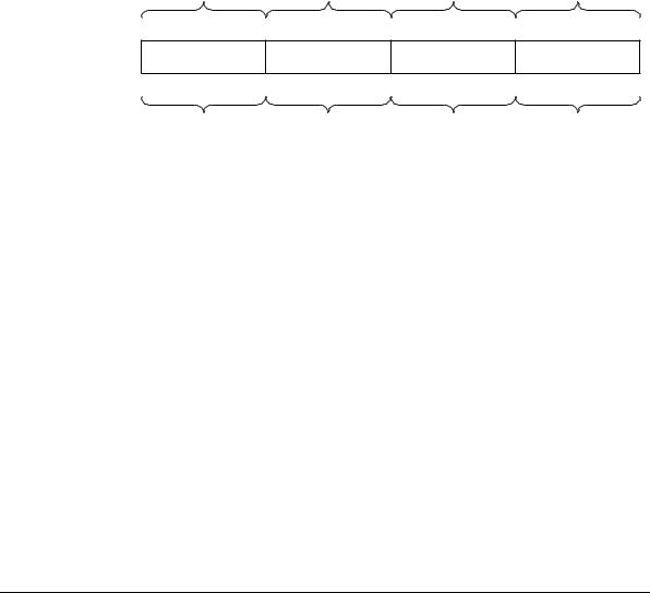
The MMCIPCellID0-3 registers are four 8-bit registers, that span address locations 0xFF0-0xFFC. The read-only registers can conceptually be treated as a single 32-bit register. The register is used as a standard cross-peripheral identification system. Figure 3-2 shows the bit assignment for the MMCIPCellID0-3 registers.
Actual register bit assignment
MMCIPCellID3 |
|
|
MMCIPCellID2 |
|
MMCIPCellID1 |
|
MMCIPCellID0 |
7 |
0 |
7 |
0 |
7 |
0 |
7 |
0 |
31 |
24 23 |
16 15 |
8 |
7 |
0 |
||
MMCIPCellID3 |
|
|
MMCIPCellID2 |
|
MMCIPCellID1 |
|
MMCIPCellID0 |
Conceptual register bit assignment
Figure 3-2 PrimeCell identification register bit assignment
The four, 8-bit registers are described in the following subsections:
•MMCIPCellID0 register
•MMCIPCellID1 register on page 3-21
•MMCIPCellID2 register on page 3-21
•MMCIPCellID3 register on page 3-21.
MMCIPCellID0 register
The MMCIPCellID0 register is hard coded and the fields within the registers determine the reset value. Table 3-24 shows the bit assignment of the MMCIPCellID0 register.
|
|
|
Table 3-24 MMCIPCellID0 register |
|
|
|
|
Bits |
Name |
Type |
Function |
|
|
|
|
31:8 |
- |
- |
Reserved, read undefined, must be written as zeros. |
|
|
|
|
7:0 |
MMCIPCellID0 |
Read |
These bits read back as 0x0D. |
|
|
|
|
3-20 |
Copyright © 2000, 2001 ARM Limited. All rights reserved. |
ARM DDI 0205B |

Programmer’s Model
MMCIPCellID1 register
The MMCIPCellID1 register is hard coded and the fields within the registers determine the reset value. Table 3-25 shows the bit assignment of the MMCIPCellID1 register.
|
|
|
Table 3-25 MMCIPCellID1 register |
|
|
|
|
Bits |
Name |
Type |
Function |
|
|
|
|
31:8 |
- |
- |
Reserved, read undefined, must be written as zeros. |
|
|
|
|
7:0 |
MMCIPCellID1 |
Read |
These bits read back as 0xF0. |
|
|
|
|
MMCIPCellID2 register
The MMCIPCellID2 register is hard coded and the fields within the registers determine the reset value. Table 3-26 shows the bit assignment of the MMCIPCellID2 register.
|
|
|
Table 3-26 MMCIPCellID2 register |
|
|
|
|
Bits |
Name |
Type |
Function |
|
|
|
|
31:8 |
- |
- |
Reserved, read undefined, must be written as zeros. |
|
|
|
|
7:0 |
MMCIPCellID2 |
Read |
These bits read back as 0x05. |
|
|
|
|
MMCIPCellID3 register
The MMCIPCellID3 register is hard coded and the fields within the registers determine the reset value. Table 3-27 shows the bit assignment of the MMCIPCellID3 register.
|
|
|
Table 3-27 MMCIPCellID3 register |
|
|
|
|
Bits |
Name |
Type |
Function |
|
|
|
|
31:8 |
- |
- |
Reserved, read undefined, must be written as zeros. |
|
|
|
|
7:0 |
MMCIPCellID3 |
Read |
These bits read back as 0xB1. |
|
|
|
|
ARM DDI 0205B |
Copyright © 2000, 2001 ARM Limited. All rights reserved. |
3-21 |

Programmer’s Model
3-22 |
Copyright © 2000, 2001 ARM Limited. All rights reserved. |
ARM DDI 0205B |