

Digital Design VHDL Laboratory
1.VHDL - Hardware Design Software Approach
pepe, 5/23/96
Programmable Combinational Logic
PAL's Programming Points
PLA's |
Programming |
Points |
PROM's Programming Points
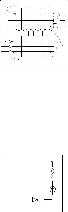
Figure 1-3. PLD Circuit Structure
Most of the time, a digital hardware designer doesn’t need to know the circuit structure of the programmable logic device (PLD) that he is using except he is conscious about the design’s speed and capacity. For example, he might want to try to “fit” a large piece of circuit into a given PLD or to select a type of fast PLD to meet a timing limit. Digital hardware can be programmed to fit a circuit into a PLD using hardware programming languages such as CUPL, Abel, PALism, and VHDL.
For more complex PLDs (CPLDs), memory elements such as flip flop devices are involved and they will be introduced later.
1.2 Problems
1)Binary Coded Decimal (BCD) is a useful decimal number representation using binary numbers. Many times, it is the only representation that digital hardware uses to communicate with humans since humans are custom to the decimal numbering system. One example is to use BCD to control the decimal LED display panel of a calculator. Each LED decimal digit has eight segments and each segment contains an LED source as shown in Figure 1-4.
+5 V
Input
Figure 1-4. LED Control Circuit
At high input “1”, current flows through the LED and resistor, and the LED glows. The typical current is about 20mA, and voltage drops 1.6 Volts(V) across the LED and 3 V across the resistor. If input is low “0”, no current will flow through LED and it will become dim.
The LED segment specification is illustrated in Figure 1-5.
10
Copyright 1996, CERL / EE, V1.00
Digital Design VHDL Laboratory
1.VHDL - Hardware Design Software Approach
pepe, 5/23/96
a
f  g
g  b
b
e |
|
|
|
|
|
c |
|
|
|
|
|
||
|
|
|
|
|
||
|
|
|
|
|||
|
|
|
|
|
||
|
|
|
d |
|||
Figure 1-5. LED Segment Control Label
The input consists of 5 bits, and the output consists of 7 bits. Out of 5 input bits, 4 bits are used to specify binary value, and one bit is used to blank all LED segments. For all output bits, one bit is used for controlling each of the segment, and one bit is used to indicate overflow of the input binary number, for example binary input greater than 9. The LED logic specification is shown in Table 1-1.
An LED segment control decoder is used to control a one-digit LED display panel. Construct such a decoder using VHDL. This can be done using if statements nested inside of a process statement or when statements alone. The form of such decoder could look like the VHDL code segment in Listing 1-3.
entity XXX is port( .... );
end XXX;
architecture XXXX of XXX is begin
-- option 1
option1: process ( input) begin
if <condition> then <output> <= <input>;
elsif <condition> then <output> <= <input>;
.....
else
<output> <= <input>; end if;
end process option1;
-- Or use option 2
output <= <input> when <condition> else <input> when <condition> else
.....
<input> when <condition> else <input>;
end XXXX;
Listing 1-3. Example VHDL Code
After completing the implementation, test the decoder for various inputs and simulate the resulting output using the NOVA simulator. The simulation session can be saved into the trace file with the “PSD” extension. This is done by using the mouse to select FILE and then Write Trace (*.PSD) on the top of the NOVA menu bar. In the saved PSD file, annotate the clock tick that corresponds to the decoder action. For example, the input that leads to the output display.
11
Copyright 1996, CERL / EE, V1.00

Digital Design VHDL Laboratory 1.VHDL - Hardware Design Software Approach pepe, 5/23/96
INPUT |
|
|
|
|
|
|
|
|
|
|
|
OUTPUT |
|
|
|
|
|
|
|
|
|
|
|
|
|
|
|
|
|
|
|
|
|
|
|
|
|
|
|
|
|
|
|
|
|
|
|
|
|
|
|
Comment |
|
Blank |
|
in1 |
|
in2 |
|
in3 |
|
in4 |
|
Overflow |
a |
|
b |
|
c |
|
d |
|
e |
|
f |
|
g |
Blank |
1 |
|
x |
|
x |
|
x |
|
x |
0 |
1 |
1 |
1 |
1 |
1 |
1 |
1 |
||||||||
0 |
0 |
0 |
0 |
0 |
0 |
0 |
0 |
0 |
0 |
0 |
0 |
0 |
1 |
||||||||||||
1 |
0 |
0 |
0 |
0 |
1 |
0 |
1 |
0 |
0 |
1 |
1 |
1 |
1 |
||||||||||||
2 |
0 |
0 |
0 |
1 |
0 |
0 |
0 |
0 |
1 |
0 |
0 |
1 |
0 |
||||||||||||
3 |
0 |
0 |
0 |
1 |
1 |
0 |
0 |
0 |
0 |
0 |
1 |
1 |
0 |
||||||||||||
4 |
0 |
0 |
1 |
0 |
0 |
0 |
1 |
0 |
0 |
1 |
1 |
0 |
0 |
||||||||||||
5 |
0 |
0 |
1 |
0 |
1 |
0 |
0 |
1 |
0 |
0 |
1 |
0 |
0 |
||||||||||||
6 |
0 |
0 |
1 |
1 |
0 |
0 |
0 |
1 |
0 |
0 |
0 |
0 |
0 |
||||||||||||
7 |
0 |
0 |
1 |
1 |
1 |
0 |
0 |
0 |
0 |
1 |
1 |
1 |
1 |
||||||||||||
8 |
0 |
1 |
0 |
0 |
0 |
0 |
0 |
0 |
0 |
0 |
0 |
0 |
0 |
||||||||||||
9 |
0 |
1 |
0 |
0 |
1 |
0 |
0 |
0 |
0 |
1 |
1 |
0 |
0 |
||||||||||||
a |
0 |
1 |
0 |
1 |
0 |
1 |
0 |
0 |
0 |
0 |
0 |
1 |
0 |
||||||||||||
b |
0 |
1 |
0 |
1 |
1 |
1 |
1 |
1 |
0 |
0 |
0 |
0 |
0 |
||||||||||||
c |
|
|
|
|
|
|
|
|
|
|
|
0 |
|
|
|
|
|
|
|
|
|
|
|
|
|
0 |
1 |
1 |
0 |
0 |
1 |
1 |
1 |
0 |
0 |
0 |
1 |
||||||||||||||
d |
|
|
|
|
|
|
|
|
|
|
|
1 |
|
|
|
|
|
|
|
|
|
|
|
|
|
0 |
1 |
1 |
0 |
1 |
1 |
0 |
0 |
0 |
0 |
1 |
0 |
||||||||||||||
e |
|
|
|
|
|
|
|
|
|
|
|
0 |
|
|
|
|
|
|
|
|
|
|
|
|
|
0 |
1 |
1 |
1 |
0 |
1 |
0 |
1 |
0 |
0 |
0 |
0 |
||||||||||||||
f |
|
|
|
|
|
|
|
|
|
|
|
0 |
|
|
|
|
|
|
|
|
|
|
|
|
|
|
0 |
|
1 |
|
1 |
|
1 |
|
1 |
1 |
|
1 |
|
1 |
|
1 |
|
0 |
|
0 |
|
0 |
|||
Table 1-1. LED-Control Truth Table
12
Copyright 1996, CERL / EE, V1.00