

page 16
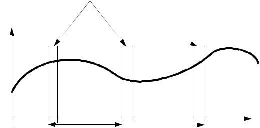
Voltage is sampled during these time periods
voltage |
time |
(Sampling Frequency)-1 |
Sampling time |
4.2.1 Analog to Digital Conversion
•When there are analog values outside a computer, and we plan to read these to digital values, there are a variety of factors to consider,
-when the sample is requested, a short period of time passes before the final sample value is obtained.
-the sample value is ‘frozen’ after a sample interval.
-after the sample is taken, the system may change
-sample values can be very sensitive to noise
-the continuous values of the signal loose some accuracy when conversion to a digital number
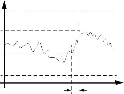
•Consider the conversion process pictured below,
page 17
V( t) |
|
|
Vmax |
V2 |
|
V1 |
|
|
Vmin |
|
t |
|
τ |
t1 |
t2 |
where, |
|
V( t) |
= |
the actual voltage over time |
|
τ |
= |
sample interval for A/D converter |
|
t |
= time |
||
t1, t2 |
= |
time at start,end of sample |
|
V1, V2 |
= voltage at start, end of sample |
||
Vmin, Vmax = input voltage range of A/D converter
N= number of bits in the A/D converter
•Once this signal is processes through a typical A/D converter we get the following relations (these may vary slightly for different types of A/D converters).
page 18
R = 2N
|
|
|
V2 |
– Vmin |
|
|
|
|
|||
VD = INT |
|
|
R – 0.5 |
|
|||||||
|
---------------------------- |
|
|||||||||
|
|
|
V |
|
|
– V |
|
|
|
|
|
|
|
|
|
max |
|
min |
|
|
|
||
|
|
|
|
|
|
|
|
||||
VERROR = |
|
Vmax |
– Vmin |
|
|
|
|||||
---------------------------- |
|
|
|
||||||||
|
|
|
|
2R |
|
|
|
|
|
||
where, |
|
|
|
|
|
|
|
|
|
|
|
R = |
resolution of A/D converter |
||||||||||
VD = |
|
the integer value of the voltage |
|||||||||
VERROR = |
the maximum quantization error |
||||||||||
•In most applications a sample is taken at regular intervals, with a period of ‘T’ seconds.
•In practice the sample interval is kept as small as possible. (i.e., tau << T)
•If we are sampling a periodic signal that changes near or faster that the sampling rate, there is a chance that we will get a signal that appears chaotic, or seems to be a lower frequency. This phenomenon is known as aliasing.
•Quite often an A/D converter will multiplex between various inputs. As it switches the voltage will be sampled by a ‘sample and hold circuit’. This will then be converted to a digital value. The sample and hold circuits can be used before the multiplexer to collect data values at the same instant in time.
4.2.1.1 - Flash A/D Converter
• On type of A/D converter is the flash converter shown below,