


78 RF CMOS POWER AMPLIFIERS:THEORY,DESIGN AND IMPLEMENTATION
the cascode transistor in the output stage acts as a resistor in series with the main amplifier, thus lowering the expected efficiency.
The design of the PA proceeds as in section 4.2. The class AB output stage is designed first such that it is capable of delivering more than 20dBm, assuming that around 2dBm of power will be lost due to the effect of the board, and package. The cascode transistor is made as wide as possible to satisfy the compromise of having lower resistive effect, and at the same time, a reasonable drain capacitance at the output node that can be absorbed by a realizable inductance value.
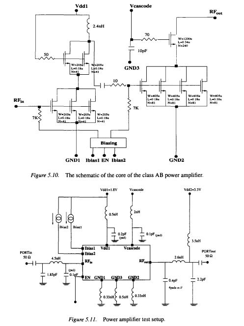
The same steps of determining the optimum load are used. The first stage is designed to provide adequate gain to drive the output stage. The interstage- matching network is completely implemented on chip due to the availability of characterized inductors. Figure 5.10 shows the core of the amplifier consisting of gain stage, output class AB stage, and the bias circuit. It is worth noting that biasing is implemented using current rather than voltage to keep the parameters of the amplifier as constant as possible with temperature and process variation. A shutdown switch is also added.
After adding the effect of the pads and the bond-wire inductances, the stability of the amplifier was greatly affected. Several resistances were added to bring the k-factor above 1 for all frequencies. The core of the amplifier, together with the bond-wires, pads, and input-output matching are shown in
Figure 5.11.
3.Simulations Results
The amplifier has been tested under typical, fast, and slow processes in order
to guarantee its full functionality. The dc operating conditions under which the amplifier is tested are shown in Table 5.1, and the input signal level, and frequency are shown in Table 5.2.
A Complete Bluetooth PA Solution |
79 |
3.1Large Signal Simulations
The power amplifier is tested for satisfying the required output power within the band of interest by applying an input power signal of 4dBm, and measuring

80 RF CMOS POWER AMPLIFIERS:THEORY,DESIGN AND IMPLEMENTATION
the output power at the 50-Ohm port. Figure 5.12 shows the variation of output power and efficiency versus the input signal frequency.
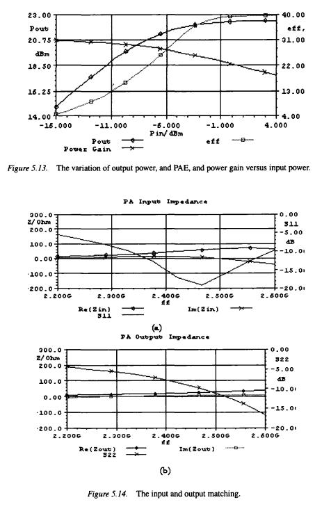
In order to test the linearity of the power amplifier, the input signal power is swept from -16dBm to 4dBm, and both the output power, and efficiency are plotted as a function of the input power in Figure 5.13. Figure 5.13 also shows the variation of the large signalgain as a function of input power. The PA gain drops from 31dB at small signal to reach 18.4dB at 4dBm input power.
The level of input, and output matching is also dependent on the input power.
In fact, variation in input power will cause a shift in the level, and frequency of the matching point. The large signal input and output matching were tested at input power of 4dBm using Harmonic Balance Simulations, in a way similar to its measurement technique using the network analyzer. The input and output impedances are measured by applying a signal of known amplitude, and measuring the input and output currents when the other port is matched. Using the equations relating the S-parameters to the Z-parameters,  and
and  are plotted as a function of frequency as shown in Figure 5.14. Table 5.3 summa- rizes the results of harmonic balance simulations at different process Corners.
A Complete Bluetooth PA Solution |
81 |