

J Comput Electron
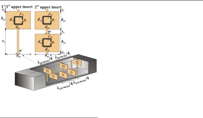
Fig. 10 3D model of the conventional H -plane dual-band bandstop Þlter using SRR
Table 4 Dimensions of the SRRs and inserts used for the design of Band I
Resonating insert |
d3i (mm) |
|
d4i (mm) |
c2i (mm) |
pi (mm) |
||
1st/3rd (i = 1, 3) |
2 |
|
4.36 |
0.3 |
0.9 |
|
|
2nd (i = 2) |
|
2 |
|
4.36 |
0.3 |
0.9 |
|
Size (mm) |
ap1 |
bp1 |
s1 |
s2 |
s3 |
s4 |
w |
|
7 |
4 |
1 |
5.16 |
0.5 |
1.16 |
2 |
|
|
|
|
|
|
|
|
4.1 Design of DBBWF
3D model of DBBWF is shown in Fig. 10. SRRs for the speciÞed stopband are inserted transversely at the appropriate positions within a rectangular waveguide. For the design of Band I, SRRs are separated by the waveguide section of length λg8.90GHz/4 = 12.469 mm, to implement inverter for the considered center frequency.
SRRs for different stopbands are distanced by (λg8.90GHz− λg10.90GHz)/4 = 3.854 mm. Dimensions for Band I are given in Table 4, while the dimensions for Band II remain unchanged and they are given in Table 2.
4.2 Miniaturization of DBBWF
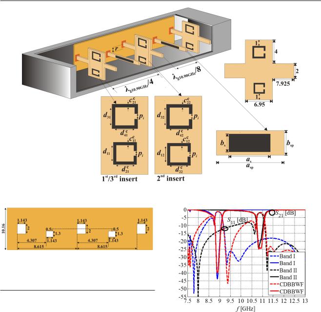
Miniaturization of DBBWF is achieved by the use of a shorter inverter for Band I, instead of the conventional quarter-wave transformer. 3D model of the compact Þlter, referred to as CDBBWF, is shown in Fig. 11.
The main beneÞts of the presented design are a smaller length of the Þlter, ßexible control of the designed stopbands and preservation of the characteristics of DBBWF.
An efÞcient way to enable all of the above-mentioned properties is to combine the miniaturization technique and the proposed algorithm.
From the design point of view, it is necessary to reduce the size of the Þlter, but to avoid the undesirable mutual coupling between the SRRs on the insert and the unwanted coupling between the additional insert and the each of the SRRs, as well. In the following, the complete set of steps relevant for the design of CDBBWF are described.
Insert geometry is chosen for the purpose of fabrication simplicity. SRRs are printed on the rectangular dielectric plate with extensions in the shape of Þn that are oriented to the lateral waveguide walls. Dimensions of the insert (in mm) are given in Fig. 11. Dimensions of the used SRRs for both stopbands given in Table 5. Some of them are adjusted for the purpose of preserving the characteristics of DBBWF, while the other dimensions remain unchanged and they are given in Tables 2 and 4.
The length of the waveguide section acting as the inverter for Band I is reduced by inserting necessary supplementary impedance, provided by properly designed additional insert placed in the middle of the waveguide section. The insert extends between the lateral waveguide walls, having dimensions asp = 22.86 mm and bsp = 1.3 mm. Dimensions of the conductive strip printed on the insert are as = 15.1 mm and bs = 0.5 mm.
To provide ßexible control of the designed stopbands, the undesirable coupling is prevented. This was done in two ways: Þrst, by increasing the interspace between the SRRs on the insert and by Þnding the optimum position of the additional insert for the inverter shortening.
The SRRs for different stopbands that are printed on the same insert are transformed into rectangular shape to increase the interspace between them, as imposed by the proposed algorithm. The SRRs are printed at 1 mm from the upper and lower edge of the insert (Fig. 11), to obtain the maximum interspace and avoid the unwanted mutual coupling between them. Further, the unwanted coupling between each of the SRRs and an additional insert for the inverter miniaturization is eliminated when the optimum position of the insert is found to be r = 0.5 mm down from the center of the transverse plane of the waveguide.
In order to ensure precise positioning of the inserts within rectangular waveguide, a supporting structure is designed. Layout of the supporting structure, along with the associated dimensions (in mm), is shown in Fig. 12.
The structure is implemented using FR-4 substrate with thickness h = 0.8 mm, relative dielectric permittivity of 4.4 and tanδ of 0.02. It is in the form of the dielectric plate with holes of proper size. Major holes are made so inserts with SRRs can be held Þrmly in place. Between these holes, minor holes were made to tightly Þx the additional insert for the inverter miniaturization.
123
J Comput Electron
Fig. 11 3D model of the third-order H -plane CDBBWF
Fig. 12 Dielectric plate with properly designed holes used as supporting structure for the positioning of the inserts within waveguide
Table 5 Dimensions of the SRRs used for the design of CDBBWF
Resonating insert |
Band II |
|
|
Band I |
|
|
|
||
|
|
|
|
|
|
|
|
|
|
|
|
dc (mm) |
cc |
(mm) |
dc (mm) |
cc |
(mm) |
||
|
|
2i |
1i |
|
|
4i |
2i |
|
|
1st/3rd (i = 1, 3) |
3.33 |
0.2 |
|
4.52 |
0.2 |
|
Fig. 13 Comparison of the frequency responses for CDBBWF and |
||
2nd (i = 2) |
3.33 |
0.16 |
4.52 |
0.2 |
|
||||
|
single-band Þlters for design of Band I and Band II |
||||||||
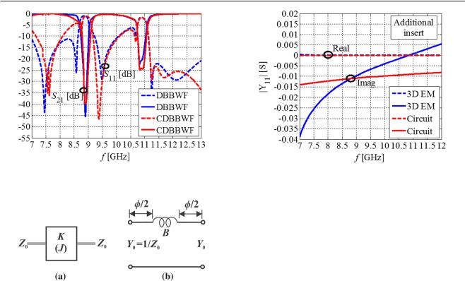
The frequency response of the proposed CDBBWF is compared with the response of each of single-band Þlters used for the design of Band I and Band II (Fig. 13). It can be observed that the unwanted mutual coupling is eliminated, so both of the stopbands of equal bandwidths can be separately controlled. Additionally, in Fig. 14, the obtained response of CDBBWF is compared with the response of DBBWF.
Total length of CDBBWF is 0.34 λg, where λg denotes the guided wavelength at the lower center frequency. The potential for further miniaturization of the proposed design is foreseen as subsequent reduction in length of the inverter
section. Drawing upon single-band bandstop Þlter design presented in [33], around 50% of size reduction can be achieved by using shorter inverter instead of conventional quarter-wave inverter.
Compared to the H -plane dual-band bandstop Þlters with independently tunable stopbands, which are DBBWF designed herein and Þlter using conventional quarter-wave inverter [34], proposed CDBBWF is signiÞcantly improved in terms of compactness. DBBWF and Þlter proposed in [34] are of lengths of 0.5 λg, while CDBBWF is 32% smaller in length.
123
J Comput Electron
Fig. 14 Comparison of the frequency responses for DBWWF and CDBBWF
Fig. 16 Comparison of the admittance parameter of the 3D EM model of the additional insert and its lumped element representation
Fig. 15 a Immittance inverter. b Realization of the immittance inverter using a lumped element and two transmission line sections
As for the E-plane Þlters having the same functionality of two individually tunable stopbands as our CDBBWF, comparison can be conducted concerning length of the Þlter. Proposed CDBBWF is more compact than the miniaturized Þlter presented in [26] of length of 0.512 λg, and the W-band Þlter of length of 0.805 λg, presented in [23].
4.3 Equivalent electrical circuit of CDBBWF
As previously discussed, the immittance inverter realized using a quarter-wavelength waveguide section is replaced with the miniaturized one. Immittance inverter denotes either the impedance inverter (K ) or admittance inverter ( J ), and it is shown in Fig. 15a. An idealized admittance inverter is a two-port network which exhibits a property at all frequencies that if it is terminated in an admittance Y2 on one port, the admittance Y1 seen looking in at the other port is:
Y1 = J 2 Y2, |
(7) |
where J is real and deÞned as the characteristic admittance of the inverter [38]. The ABCD matrix of an ideal admittance inverter is:
A |
B |
|
0 |
± |
1 |
. |
|
|
j J |
(8) |
|||||||
C |
D = |
|
|
j J |
0 |
|
|
|
|
|
|
|
|||||
The simplest realization of inverter is a quarter-wave transmission line. Besides that, immittance inverter can also be realized using lumped and transmission-line elements, as shown in Fig. 15b.
The symbol B denotes the susceptance of the lumped element, while Y0 and φ denote the characteristic admittance and electrical length of the line, respectively. It is characterized by the following equations:
B = −1/(ωL) |
(9) |
J = Y0 tan |φ/2| |
(10) |
φ = − tan−1 (2B/Y0) |
(11) |
|B/Z0| = ( J/Y0) 1 − ( J/Y0)2 . |
(12) |
To develop an equivalent circuit of CDBBWF, it is necessary to Þnd the value of the lumped element used for the representation of the additional insert. Based on the 3D EM analysis of the additional insert, inductive behavior is observed at particular frequency of 8.90 GHz. After substitution of the value of the susceptance B obtained by the 3D EM analysis into Eq. 9, the value of the inductance is calculated. Comparison of the admittance parameter for the 3D EM model of the additional insert and its lumped element representation is given in Fig. 16.
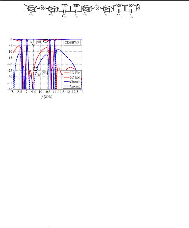
Equivalent electrical circuit of CDBBWF is shown in Fig. 17. Inductor with inductance Ls is used to represent the additional insert at the circuit level. Waveguide sections are of length Ds, which is equal to Ds = λg10.90GHz/8 = 4.3075 mm. Ports impedances are set to 502 , which is the value of the waveguide impedance for 9.90 GHz (the frequency between the considered ones).
Comparison of the frequency responses for the 3D EM model of CDBBWF and its equivalent electrical circuit is presented in Fig. 18. Values of the equivalent circuit elements are given in Table 6.
123
J Comput Electron
Fig. 17 Equivalent electrical circuit of CDBBWF
Fig. 18 Comparison of the frequency responses for CDBBWF and its equivalent electrical circuit
The Þlter responses for DBBWF, CDBBWF and its electrical circuit are numerically compared in Table 7. According to the results given in Table 7, very good agreement can be observed between the responses in terms of center frequencies and bandwidths of the designed stopbands.
5 Experimental veriÞcation
The experimental setup employed for the measurement is Agilent N5227A PNA network analyzer, covering the frequency range from 10 MHz to 67 GHz. Two WR-90 to SMA female waveguide to coax adapters are used for transitions from waveguide to 50coaxial line. The network analyzer is conÞgured to measure frequency response over the fre-
Table 6 Values of equivalent circuit elements for CDBBWF
quency band of 8.2Ð12.4 GHz (X-band), which is a speciÞed operating range of the WR-90 rectangular waveguide. The photograph of the fabricated Þlter is given in Fig. 19.
To ensure the adequate measurement of the fabricated Þlter prototype, the effect of manufacturer dielectric permittivity tolerance is investigated. The manufacturerÕs speciÞcation indicates that the nominal value of the relative dielectric permittivity with the associated tolerance is εr = 2.65 ± 0.05. The exact value of the dielectric permittivity of the substrate is determined from the measurements of insert with single SRR and is found to be equal to 2.70. After performing precise measurements of the physical dimensions, it was determined that the fabricated SRRs for Band I are less than 20 μm wider than the simulated ones.
Therefore, additional 3D EM simulations are performed to include the increased value of the SRR width and the exact value of the dielectric permittivity. Due to a small tolerancerelated change of the dielectric permittivity of the substrate, the center frequencies of the Þlter are targeted at 8.85 and 10.85 GHz. Band I is slightly wider than Band II, because of the minor change in width of the fabricated SRRs.
In our study, the conductivity parameter in 3D EM simulations was initially set to 20 MS/m. The estimate is obtained based on a set of results of the measurements that authors have performed previously. In that manner, after the fabrication and measurement of the considered Þlter, better insight into impact of losses on the measured Þlter response can be obtained, while the modeled losses can be modiÞed appropriately in simulations performed after the measurements. Accordingly, additional simulations were carried out including higher conductivity value than the initially set 20 MS/m. For the post-measurement analysis of the considered dual-
Parameter |
L11 (nH) |
L12 (nH) |
L21 (nH) |
L22 (nH) |
Ls (nH) |
C11 (pF) |
C12 (pF) |
C21 (pF) |
C22 (pF) |
Value |
0.546 |
0.668 |
0.387 |
0.360 |
1.49 |
0.587 |
0.499 |
0.549 |
0.599 |
|
|
|
|
|
|
|
|
|
|
Table 7 Comparison of the Þlter responses and overall lengths
Filter type |
f01 (GHz) |
B3dB1 (MHz) |
f02 (GHz) |
B3dB2 (MHz) |
Length |
CDBBWF |
8.90 |
340 |
10.90 |
340 |
0.34 λg |
DBBWF |
8.90 |
342 |
10.90 |
340 |
0.5 λg |
Equivalent circuit of |
8.92 |
341 |
10.91 |
342 |
Ð |
CDBBWF |
|
|
|
|
|
|
|
|
|
|
|
123