


Table A-5 Peripheral Port Timing
VDD = 5.0 Vdc ±10%, VSS = 0 Vdc, TA = TL to TH |
|
|
|
|
|
|
||||
|
|
|
|
|
|
|
|
|
|
|
Characteristic |
Symbol |
1.0 MHz |
2.0 MHz |
3.0 MHz |
Unit |
|
||||
|
|
|
|
|
|
|
|
|
|
|
|
|
Min |
Max |
Min |
Max |
Min |
|
Max |
|
|
|
|
|
|
|
|
|
|
|
|
|
Frequency of Operation (E-Clock Frequency) |
fo |
dc |
1.0 |
dc |
2.0 |
dc |
|
3.0 |
MHz |
|
E-Clock Period |
tcyc |
1000 |
— |
500 |
— |
333 |
|
— |
ns |
|
Peripheral Data Setup Time |
tPDSU |
100 |
— |
100 |
— |
100 |
|
— |
ns |
|
MCU Read of Ports A, C, D, and E |
|
|
|
|||||||
|
|
|
|
|
|
|
|
|
|
|
Peripheral Data Hold Time |
tPDH |
50 |
— |
50 |
— |
50 |
|
— |
ns |
|
MCU Read of Ports A, C, D, and E |
|
|
|
|||||||
|
|
|
|
|
|
|
|
|
|
|
Delay Time, Peripheral Data Write |
tPWD |
— |
200 |
— |
200 |
— |
|
200 |
ns |
|
MCU Write to Port A |
|
|
|
|||||||
MCU Writes to Ports B, C, and D |
|
— |
350 |
— |
225 |
— |
|
183 |
ns |
|
tPWD = 1/4 tcyc + 100 ns |
|
|
|
|
|
|
|
|
|
|
Input Data Setup Time (Port C) |
tIS |
60 |
— |
60 |
— |
60 |
|
— |
ns |
|
Input Data Hold Time (Port C) |
tIH |
100 |
— |
100 |
— |
100 |
|
— |
ns |
A |
Delay Time, E Fall to STRB |
tDEB |
— |
350 |
— |
225 |
— |
183 |
ns |
||
tDEB = 1/4 tcyc + 100 ns |
|
|
|
|
|
|
|
|
|
|
Setup Time, STRA Asserted to E Fall (Note 1) |
tAES |
0 |
— |
0 |
— |
0 |
|
— |
ns |
|
Delay Time, STRA Asserted to Port C Data Output |
t |
— |
100 |
— |
100 |
— |
100 |
ns |
||
Valid |
PCD |
|
|
|
|
|
|
|
|
|
|
|
|
|
|
|
|
|
|
|
|
Hold Time, STRA Negated to Port C Data |
tPCH |
10 |
— |
10 |
— |
10 |
|
— |
ns |
|
Three-State Hold Time |
tPCZ |
— |
150 |
— |
150 |
— |
150 |
ns |
|
|
NOTES:
1.If this setup time is met, STRB acknowledges in the next cycle. If it is not met, the response may be delayed one more cycle.
2.Port C and D timing is valid for active drive (CWOM and DWOM bits not set in PIOC and SPCR registers respectively).
3.All timing is shown with respect to 20% VDD and 70% VDD, unless otherwise noted.
M68HC11 E SERIES |
ELECTRICAL CHARACTERISTICS |
MOTOROLA |
TECHNICAL DATA |
|
A-11 |
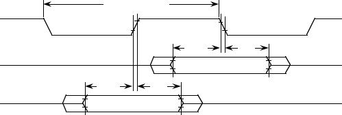
Table A-5a Peripheral Port Timing (MC68L11E9)
VDD = 3.0 Vdc to 5.5 Vdc, VSS = 0 Vdc, TA = TL to TH
|
Characteristic |
Symbol |
1.0 MHz |
2.0 MHz |
Unit |
||
|
|
|
|
|
|
|
|
|
|
|
Min |
Max |
Min |
Max |
|
|
|
|
|
|
|
|
|
|
Frequency of Operation (E-Clock Frequency) |
fo |
dc |
1.0 |
dc |
2.0 |
MHz |
|
E-Clock Period |
tcyc |
1000 |
— |
500 |
— |
ns |
|
Peripheral Data Setup Time |
tPDSU |
100 |
— |
100 |
— |
ns |
|
MCU Read of Ports A, C, D, and E |
|
|||||
|
|
|
|
|
|
|
|
|
Peripheral Data Hold Time |
tPDH |
50 |
— |
50 |
— |
ns |
|
MCU Read of Ports A, C, D, and E |
|
|||||
|
|
|
|
|
|
|
|
|
Delay Time, Peripheral Data Write |
tPWD |
— |
250 |
— |
250 |
ns |
|
MCU Write to Port A |
|
|||||
|
MCU Writes to Ports B, C, and D |
|
— |
400 |
— |
275 |
ns |
|
tPWD = 1/4 tcyc + 150 ns |
|
|
|
|
|
|
|
Input Data Setup Time (Port C) |
tIS |
60 |
— |
60 |
— |
ns |
A |
Input Data Hold Time (Port C) |
tIH |
100 |
— |
100 |
— |
ns |
Delay Time, E Fall to STRB |
tDEB |
— |
400 |
— |
275 |
ns |
|
tDEB = 1/4 tcyc + 150 ns |
|
|
|
|
|
|
|
Setup Time, STRA Asserted to E Fall (Note 1) |
tAES |
0 |
— |
0 |
— |
ns |
|
Delay Time, STRA Asserted to Port C Data Output Valid |
tPCD |
— |
100 |
— |
100 |
ns |
|
|
Hold Time, STRA Negated to Port C Data |
tPCH |
10 |
— |
10 |
— |
ns |
|
Three-State Hold Time |
tPCZ |
— |
150 |
— |
150 |
ns |
NOTES:
1.If this setup time is met, STRB acknowledges in the next cycle. If it is not met, the response may be delayed one more cycle.
2.Port C and D timing is valid for active drive (CWOM and DWOM bits not set in PIOC and SPCR registers respectively).
3.All timing is shown with respect to 20% VDD and 70% VDD, unless otherwise noted.
MCU READ OF PORT |
|
|
E |
|
|
|
tPDSU |
tPDH |
PORTS |
|
|
A, C*, D |
|
|
tPDSU |
tPDH |
|
PORT E
* FOR NON-LATCHED OPERATION OF PORT C
E9 PORT RD TIM
Figure A-7 Port Read Timing Diagram
MOTOROLA |
ELECTRICAL CHARACTERISTICS |
M68HC11 E SERIES |
A-12 |
|
TECHNICAL DATA |
|
MCU WRITE TO PORT |
|
|
E |
|
|
|
|
tPWD |
|
|
PORTS |
PREVIOUS PORT DATA |
NEW DATA VALID |
|
B, C, D |
|||
|
|
||
|
|
tPWD |
PORT A |
PREVIOUS PORT DATA |
NEW DATA VALID |
E9 PORT WR TIM
Figure A-8 Port Write Timing Diagram
STRA (IN)
 tIS
tIS 
 tIS
tIS 
A
PORT C (IN)
SIMPLE INPUT STROBE TIM
Figure A-9 Simple Input Strobe Timing Diagram
|
MCU WRITE TO PORT B |
|
E |
|
|
|
tPWD |
|
PORT B |
PREVIOUS PORT DATA |
NEW DATA VALID |
|
|
tDEB |
STRB (OUT)
SIMPLE OUTPUT STROBE TIM
Figure A-10 Simple Output Strobe Timing Diagram
M68HC11 E SERIES |
ELECTRICAL CHARACTERISTICS |
MOTOROLA |
TECHNICAL DATA |
|
A-13 |

|
READ PORTCL1 |
E |
|
tDEB |
tDEB |
"READY" |
|
STRB (OUT) |
|
tAES |
|
STRA (IN)
 tIS
tIS 
 tIH
tIH 
PORT C (IN)
NOTES:
1.After reading PIOC with STAF set
2.Figure shows rising edge STRA (EGA = 1) and high true STRB (INVB = 1).
PORT C INPUT HNDSHK TIM
A |
Figure A-11 Port C Input Handshake Timing Diagram |
|
E
PORT C (OUT)
STRB (OUT)
WRITE PORTCL1 |
|
|
tPWD |
|
|
PREVIOUS PORT DATA |
NEW DATA VALID |
|
|
tDEB |
tDEB |
|
|
"READY" |
|
|
tAES |
STRA (IN)
NOTES:
1.After reading PIOC with STAF set
2.Figure shows rising edge STRA (EGA = 1) and high true STRB (INVB = 1).
PORT C OUTPUT HNDSHK TIM
Figure A-12 Port C Output Handshake Timing Diagram
MOTOROLA |
ELECTRICAL CHARACTERISTICS |
M68HC11 E SERIES |
A-14 |
|
TECHNICAL DATA |

|
READ PORTCL1 |
|
|
|
|
|
E |
|
|
|
|
|
|
|
tPWD |
|
|
|
|
|
PORT C (OUT) |
|
|
|
|
|
|
(DDR = 1) |
|
|
|
|
|
|
|
|
t |
DEB |
"READY" |
|
tDEB |
|
|
|
|
|
||
STRB (OUT) |
|
|
|
|
|
|
|
|
|
|
|
tAES |
|
STRA (IN) |
|
|
|
|
|
|
|
tPCD |
|
|
tPCH |
|
|
PORT C (OUT) |
OLD DATA |
NEW DATA VALID |
|
|
|
|
(DDR = 0) |
|
|
A |
|||
|
|
|
|
|
||
|
a) STRA ACTIVE BEFORE PORTCL WRITE |
|
tPCZ |
|||
|
|
|
||||
|
|
|
|
|||
STRA (IN) |
|
|
|
|
|
|
|
|
|
tPCD |
tPCH |
|
|
PORT C (OUT) |
|
|
|
NEW DATA VALID |
|
|
(DDR = 0) |
|
|
|
|
|
|
|
|
|
|
|
|
|
|
b) STRA ACTIVE AFTER PORTCL WRITE |
|
tPCZ |
|
||
|
|
|
|
|||
NOTES:
1.After reading PIOC with STAF set
2.Figure shows rising edge STRA (EGA = 1) and high true STRB (INVB = 1).
3-STATE VAR OUTPUT HNDSHK TIM
Figure A-13 Three-State Variation of Output Handshake Timing Diagram
(STRA Enables Output Buffer)
M68HC11 E SERIES |
ELECTRICAL CHARACTERISTICS |
MOTOROLA |
TECHNICAL DATA |
|
A-15 |

Table A-6 Analog-To-Digital Converter Characteristics
|
VDD = 5.0 Vdc ±10%, VSS = 0 Vdc, TA = TL to TH, 750 kHz ≤E ≤3.0 MHz, unless otherwise noted |
|
|
|
||||||||
|
|
|
|
|
|
|
|
|
|
|
|
|
|
Characteristic |
Parameter |
|
Min |
Absolute |
|
|
2.0 MHz |
3.0 MHz |
|
Unit |
|
|
|
|
|
|
|
|
|
|
|
|
|
|
|
|
|
|
|
|
|
|
Max |
Max |
|
|
|
|
|
|
|
|
|
|
|
|
|
|
|
|
|
Resolution |
Number of Bits Resolved by A/D Converter |
— |
8 |
|
|
— |
— |
Bits |
|||
|
|
|
|
|
|
|
|
|
|
|
|
|
|
|
|
|
|
|
|
|
|
|
|
|
|
|
Non-Linearity |
Maximum Deviation from the Ideal A/D |
— |
— |
|
|
±1/2 |
±1 |
|
|
LSB |
|
|
|
Transfer Characteristics |
|
|
|
|
|
|
|
|
|
|
|
|
|
|
|
|
|
|
|
|
|
|
|
|
Zero Error |
Difference Between the Output of an Ideal |
— |
— |
|
|
±1/2 |
±1 |
|
|
LSB |
|
|
|
and an Actual for Zero Input Voltage |
|
|
|
|
|
|
|
|
|
|
|
|
|
|
|
|
|
|
|
|
|
|
|
|
Full Scale Error |
Difference Between the Output of an Ideal |
— |
— |
|
|
±1/2 |
±1 |
|
|
LSB |
|
|
|
and an Actual A/D for Full-Scale Input |
|
|
|
|
|
|
|
|
|
|
|
|
Voltage |
|
|
|
|
|
|
|
|
|
|
|
|
|
|
|
|
|
|
|
|
|
|
|
|
Total Unadjusted |
Maximum Sum of Non-Linearity, Zero Error, |
— |
— |
|
|
±1/2 |
±1 1/2 |
|
|
LSB |
|
|
Error |
and Full-Scale Error |
|
|
|
|
|
|
|
|
|
|
|
|
|
|
|
|
|
|
|
|
|
|
|
|
Quantization |
Uncertainty Because of Converter |
|
— |
— |
|
|
±1/2 |
±1/2 |
|
|
LSB |
A |
Error |
Resolution |
|
|
|
|
|
|
|
|
|
|
|
|
|
|
|
|
|
|
|
|
|
||
Absolute |
Difference Between the Actual Input Voltage |
— |
— |
|
|
±1 |
±2 |
|
|
LSB |
||
Accuracy |
and the Full-Scale Weighted Equivalent |
|
|
|
|
|
|
|
|
|
||
|
|
|
|
|
|
|
|
|
|
|||
|
|
of the Binary Output Code, All Error |
|
|
|
|
|
|
|
|
|
|
|
|
Sources Included |
|
|
|
|
|
|
|
|
|
|
|
|
|
|
|
|
|
|
|
|
|
|
|
|
Conversion |
Analog Input Voltage Range |
|
VRL |
— |
|
|
V RH |
VRH |
|
|
V |
|
Range |
|
|
|
|
|
|
|
|
|
|
|
|
|
|
|
|
|
|
|
|
|
|||
|
VRH |
Maximum Analog Reference Voltage |
VRL |
— |
|
V DD + 0.1 |
VDD + 0.1 |
|
V |
|||
|
|
(Note 2) |
|
|
|
|
|
|
|
|
|
|
|
|
|
|
|
|
|
|
|
|
|
|
|
|
VRL |
Minimum Analog Reference Voltage |
VSS -0.1 |
— |
|
|
V RH |
VRH |
|
|
V |
|
|
|
(Note 2) |
|
|
|
|
|
|
|
|
|
|
|
|
|
|
|
|
|
|
|
|
|
||
|
VR |
Minimum Difference between VRH and VRL |
3 |
— |
|
|
— |
— |
|
V |
||
|
|
(Note 2) |
|
|
|
|
|
|
|
|
|
|
|
|
|
|
|
|
|
|
|
|
|
|
|
|
Conversion Time |
Total Time to Perform a Single |
|
|
|
|
|
|
|
|
|
|
|
|
Analog-to-Digital Conversion: |
|
|
|
|
|
|
|
|
|
|
|
|
|
E Clock |
— |
32 |
|
|
— |
— |
t |
|
cyc |
|
|
Internal RC Oscillator |
— |
— |
t |
cyc + 32 |
tcyc + 32 |
|
µs |
|||
|
Monotonicity |
Conversion Result Never Decreases with an |
— |
Guaranteed |
|
|
— |
— |
— |
|
||
|
|
Increase in Input Voltage and has no |
|
|
|
|
|
|
|
|
|
|
|
|
Missing Codes |
|
|
|
|
|
|
|
|
|
|
|
|
|
|
|
|
|
|
|
|
|
|
|
|
Zero Input |
Conversion Result when Vin = VRL |
|
00 |
— |
|
|
— |
— |
Hex |
||
|
Reading |
|
|
|
|
|
|
|
|
|
|
|
|
|
|
|
|
|
|
|
|
|
|
|
|
|
Full Scale |
Conversion Result when Vin = VRH |
|
— |
— |
|
|
FF |
FF |
|
Hex |
|
|
Reading |
|
|
|
|
|
|
|
|
|
|
|
|
|
|
|
|
|
|
|
|
|
|
|
|
|
Sample |
Analog Input Acquisition Sampling Time: |
|
|
|
|
|
|
|
|
|
|
|
Acquisition |
|
E Clock |
— |
12 |
|
|
— |
— |
t |
|
cyc |
|
Time |
|
|
|
|
|
|
|
|
|
|
|
|
Internal RC Oscillator |
— |
— |
|
|
12 |
12 |
|
|
µs |
||
|
|
|
|
|
|
|||||||
|
|
|
|
|
|
|
|
|
|
|
|
|
|
Sample/Hold |
Input Capacitance During Sample PE[7:0] |
— |
20 (Typ) |
|
|
— |
— |
pF |
|||
|
Capacitance |
|
|
|
|
|
|
|
|
|
|
|
|
|
|
|
|
|
|
|
|
|
|
|
|
|
Input Leakage |
Input Leakage on A/D Pins |
PE[7:0] |
— |
— |
|
|
400 |
400 |
|
nA |
|
|
|
|
|
|
|
|
|
|
|
|
|
|
|
|
|
VRL, VRH |
— |
— |
|
|
1.0 |
1.0 |
|
|
µA |
|
NOTES: |
|
|
|
|
|
|
|
|
|
|
|
|
1. Source impedances greater than 10 kΩ affect accuracy adversely because of input leakage. |
|
|
|
|
|||||||
|
2. Performance verified down to 2.5 V VR, but accuracy is tested and guaranteed at |
VR = 5 V ±10%. |
|
|
|
|||||||
MOTOROLA |
ELECTRICAL CHARACTERISTICS |
M68HC11 E SERIES |
A-16 |
|
TECHNICAL DATA |
Table A-6a Analog-To-Digital Converter Characteristics (MC68L11E9)
VDD = 3.0 Vdc to 5.5 Vdc, VSS = 0 Vdc, TA = TL to TH, 750 kHz ≤E ≤2.0 MHz, unless otherwise noted
Characteristic |
Parameter |
|
Min |
Absolute |
Max |
Unit |
|
|
|
|
|
|
|
|
|
||
Resolution |
Number of Bits Resolved by A/D Converter |
— |
8 |
— |
Bits |
|
||
|
|
|
|
|
|
|
||
Non-Linearity |
Maximum Deviation from the Ideal A/D Transfer |
— |
— |
±1 |
LSB |
|
||
|
Characteristics |
|
|
|
|
|
|
|
|
|
|
|
|
|
|
||
Zero Error |
Difference Between the Output of an Ideal and an |
— |
— |
±1 |
LSB |
|
||
|
Actual for Zero Input Voltage |
|
|
|
|
|
|
|
|
|
|
|
|
|
|
||
Full Scale Error |
Difference Between the Output of an Ideal and an |
— |
— |
±1 |
LSB |
|
||
|
Actual A/D for Full-Scale Input Voltage |
|
|
|
|
|
|
|
|
|
|
|
|
|
|
||
Total Unadjusted |
Maximum Sum of Non-Linearity, Zero Error, and |
— |
— |
±1 1/2 |
LSB |
|
||
Error |
Full-Scale Error |
|
|
|
|
|
|
|
|
|
|
|
|
|
|
||
Quantization Error |
Uncertainty Because of Converter Resolution |
— |
— |
±1/2 |
LSB |
|
||
|
|
|
|
|
|
|
||
Absolute Accuracy |
Difference Between the Actual Input Voltage and |
— |
— |
±2 |
LSB |
|
||
|
the Full-Scale Weighted Equivalent of the |
|
|
|
|
|
|
|
|
Binary Output Code, All Error Sources |
|
|
|
|
|
|
|
|
Included |
|
|
|
|
|
|
A |
|
|
|
|
|
|
|
|
|
Conversion Range |
Analog Input Voltage Range |
|
VRL |
— |
V RH |
|
V |
|
VRH |
Maximum Analog Reference Voltage |
|
VRL |
— |
V DD + 0.1 |
|
V |
|
VRL |
Minimum Analog Reference Voltage |
|
VSS –0.1 |
— |
V RH |
|
V |
|
VR |
Minimum Difference between VRH and VRL |
3.0 |
— |
— |
V |
|
||
Conversion Time |
Total Time to Perform a Single |
|
|
|
|
|
|
|
|
Analog-to-Digital Conversion: |
|
|
|
|
|
|
|
|
|
E Clock |
— |
32 |
— |
t |
cyc |
|
|
Internal RC Oscillator |
— |
— |
t cyc + 32 |
|
µs |
|
|
Monotonicity |
Conversion Result Never Decreases with an |
— |
Guaranteed |
— |
— |
|
|
|
|
Increase in Input Voltage and has no Missing |
|
|
|
|
|
|
|
|
Codes |
|
|
|
|
|
|
|
|
|
|
|
|
|
|
|
|
Zero Input Reading |
Conversion Result when Vin = VRL |
|
00 |
— |
— |
Hex |
|
|
Full Scale Reading |
Conversion Result when Vin = VRH |
|
— |
— |
FF |
Hex |
|
|
Sample |
Analog Input Acquisition Sampling Time: |
|
|
|
|
|
|
|
Acquisition Time |
|
E Clock |
— |
12 |
— |
t |
cyc |
|
|
Internal RC Oscillator |
— |
— |
12 |
|
µs |
|
|
|
|
|
|
|
|
|
|
|
Sample/Hold |
Input Capacitance During Sample |
PE[7:0] |
— |
20 (Typ) |
— |
pF |
|
|
Capacitance |
|
|
|
|
|
|
|
|
|
|
|
|
|
|
|
|
|
Input Leakage |
Input Leakage on A/D Pins |
PE[7:0] |
— |
— |
400 |
nA |
|
|
|
|
|
|
|
|
|
|
|
|
|
VRL, VRH |
— |
— |
1.0 |
µA |
|
|
NOTES:
1. Source impedances greater than 10 kΩ affect accuracy adversely because of input leakage.
M68HC11 E SERIES |
ELECTRICAL CHARACTERISTICS |
MOTOROLA |
TECHNICAL DATA |
|
A-17 |