

Furber S.ARM system-on-chip architecture.2000
.pdf130 The ARM Instruction Set
Examples |
To expand an array of signed half-words into an array of words: |
||
|
ADR |
r1, ARRAYl |
; half-word array start |
|
ADR |
r2, ARRAY2 |
; word array start |
|
ADR |
r3, ENDARR1 |
; ARRAYl end + 2 |
|
LOOP LDRSH |
r0, [r1], #2 |
; get signed half-word |
|
STR |
r0, [r2], #4 |
; save word |
|
CMP |
r1, r3 |
; check for end of array |
|
BLT |
LOOP |
; if not finished, loop |
Notes |
1. Similar limitations to those on the word and unsigned byte transfers described in |
||
|
the previous section apply on the use of r15 and the register operands. |
||
2.All half-word transfers should use half-word aligned addresses.
5.12Multiple register transfer instructions
The ARM multiple register transfer instructions allow any subset (or all) of the 16 registers visible in the current operating mode to be loaded from or stored to memory. A form of the instruction also allows the operating system to load or store the user-mode registers to save or restore the user process state, and another form allows the CPSR to be restored from the SPSR as part of a return from an exception handler.
These instructions are used on procedure entry and return to save and restore workspace registers and are useful for high-bandwidth memory block copy routines.
Figure 5.11 Multiple register data transfer instruction binary encoding.
Binary encoding
Multiple register transfer instructions |
131 |
Description
Assembler format
Examples
The register list in the bottom 16 bits of the instruction includes a bit for each visible register, with bit 0 controlling whether or not r0 is transferred, bit 1 controls r1, and so on up to bit 15 which controls the transfer of the PC.
The registers are loaded from or stored to a contiguous block of memory words defined by the base register and the addressing mode. The base address will be incremented (U = 1) or decremented (U = 0) before (P = 1) or after (P = 0) each word transfer. Auto-indexing is supported; if W = 1 the base register will be increased (U = 1) or decreased (U = 0) by the number of bytes transferred when the instruction completes.
Special forms of the instruction allow it to be used to restore the CPSR: if the PC is in the register list of a load multiple and the S bit is set, the SPSR of the current mode will be copied into the CPSR, giving an atomic return and restore state instruction. This form should not be used in user mode code since there is no SPSR in user mode.
If the PC is not in the register list and the S bit is set, both load and store multiple instructions executed in non-user modes will transfer the user mode registers (while using the current mode base register). This allows an operating system to save and restore user process state.
The normal form of the instruction is:
LDMISTM{<cond>}<add mode> Rn{!}, <registers>
where odd mode> specifies one of the addressing modes detailed in Table 3.1 on page 62. The instruction bits correspond closely to the mechanistic view described in this table, with 'increment' corresponding to U = 1 and 'before' corresponding to P = 1. '!' specifies auto-indexing (W = 1), and <registers> is a list of registers and register ranges enclosed in curly brackets, for example: {r0, r3-r7, pc}.
In a non-user mode, the CPSR may be restored by: |
|
LDM{<cond>}<add mode> R n { ! } , |
<registers + pc>^ |
The register list must contain the PC. In a non-user mode, the user registers may be saved or restored by:
LDM I STM{<cond>}<add mode> Rn, <registers -
pc>~ Here the register list must not contain the PC and write-back is not
allowed.
To save three work registers and the return address upon entering a subroutine:
STMFD |
r13!, {r0-r2, r14} |
This assumes that r13 has been initialized for use as a stack pointer. To restore the work registers and return:
LDMFD r13!, |
{r0-r2, |
pc} |
|
132 The ARM Instruction Set
Notes |
1. If the PC is specified in the register list in a store multiple instruction, the value |
|
saved is implementation dependent. Normally, therefore, specifying the PC in an |
|
STM should be avoided. (Loading the PC has the expected result and is a stand |
|
ard way of returning from a procedure.) |
2.The base register may be specified in the transfer list of either a load or store mul tiple, but write-back should not be specified in the same instruction since the result of doing so is unpredictable.
3.If the base register contains an address that is not word-aligned, the bottom two bits will be ignored. Some ARM systems may generate an exception.
4.In architecture v5T only, the bottom bit of a loaded PC updates the Thumb bit.
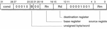
5.13Swap memory and register instructions (SWP)
Swap instructions combine a load and a store of a word or an unsigned byte in a single instruction. Normally the two transfers are combined into an atomic memory operation that cannot be split by an external memory access (for instance from a DMA controller), and therefore the instruction can be used as the basis of a semaphore mechanism to give mutually exclusive access to data structures that are shared between multiple processes, processors, or a processor and a DMA controller. These instructions are little used outside their role in the construction of semaphores.
Binary encoding
|
Figure 5.12 Swap memory and register instruction binary encoding. |
Description |
The instruction loads the word (B = 0) or unsigned byte (B = 1) at the memory loca- |
|
tion addressed by Rn into Rd, and stores the same data type from Rm into the same |
|
memory location. Rd and Rm may be the same register (but should both be distinct |
|
from Rn), in which case the register and memory values are exchanged. The ARM |
|
executes separate memory read and then memory write cycles, but asserts a 'lock' |
|
signal to indicate to the memory system that the two cycles should not be separated. |
Status register to general register transfer instructions |
133 |
Assembler |
SWP{<cond>}{B} Rd, |
Rm, |
|
format |
[Rn] |
|
|
Example |
ADR |
r0, SEMAPHORE |
; exchange byte |
|
SWPB |
r1, r1, [r0] |
|
Notes |
1. The PC should not be used as any of the registers in this instruction. |
||
2.The base register (Rn) should not be the same as either the source (Rm) or the destination (Rd) register.
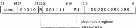
5.14Status register to general register transfer instructions
When it is necessary to save or modify the contents of the CPSR or the SPSR of the current mode, those contents must first be transferred into a general register, the selected bits modified and then the value returned to the status register. These instructions perform the first step in this sequence.
Binary encoding
Figure 5.13 Status register to general register transfer instruction binary encoding.
Description
Assembler format
Examples
The CPSR (R = 0) or the current mode SPSR (R = 1) is copied into the destination register (Rd). All 32 bits are copied.
MRS{<cond>} Rd,
CPSRISPSR
MRS |
r0, |
; move the CPSR to r0 ; |
|
CPSR |
|
move the SPSR to r3 |
|
MRS |
r3, |
||
|
|||
SPSR |
|
|
134 The ARM Instruction Set
Notes |
1. The SPSR form should not be used in user or system mode since there is no |
|
accessible SPSR in those modes. |
2.When modifying the CPSR or SPSR care should be taken to preserve the values of all the unused bits; this will maximize the probability of compatibility with future uses of those bits. This is best achieved by moving the status register to a general register (using these instructions), modifying only the necessary bits and then moving the result back to the status register.
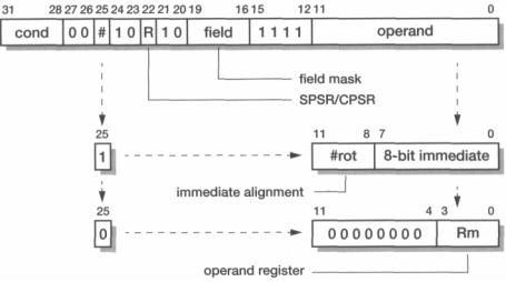
5.15General register to status register transfer instructions
When it is necessary to save or modify the contents of the CPSR or the SPSR of the current mode, those contents must first be transferred into a general register, the selected bits modified and then the value returned to the status register. These instructions perform the last step in this sequence.
Binary encoding
Figure 5.14 Transfer to status register instruction binary encoding.
General register to status register transfer instructions |
135 |
Description |
The operand, which may be a register (Rm) or a rotated 8-bit immediate (specified in the |
|||
|
same way as the immediate form of operand2 in the data processing instructions), is |
|||
|
moved under a field mask to the CPSR (R = 0) or current mode SPSR (R = I). |
|||
|
The field mask controls the update of the four byte fields within the PSR register. |
|||
|
Instruction bit 16 determines whether PSR[7:0] is updated, bit 17 controls PSR[15:8], |
|||
|
bit 18 controls PSR[23:16] and bit 19 controls PSR[31:24]. |
|
||
|
When an immediate operand is used only the flags (PSR[31:24]) may be selected |
|||
|
for update. (These are the only bits that may be updated by user-mode code.) |
|||
Assembler |
MSR{<cond>} CPSR_fISPSR_f, #<32-bit immediate> |
|||
format |
MSR{<cond>} CPSR_<field>ISPSR_<field>, Rm |
|||
|
where <f ield> is one of: |
|
|
|
|
• c - the control field - PSR[7:0]. |
|
|
|
|
• x - the extension field - PSR[15:8] (unused on current ARMs). |
|||
|
• s - the status field - PSR[23:16] (unused on current ARMs). |
|||
|
• f- the flags field -PSR[31:24]. |
|
|
|
Examples |
To set the N, Z, C and V flags: |
|
|
|
|
MSR |
CPSR_f, |
#&f0000000; |
set all the flags |
To set just the C flag, preserving N, Z and V:
MRS |
r0, |
CPSR |
movetheCPSRtor0set |
ORR |
r0, |
r0, |
bit 29 of r0 move back |
#&20000000 |
|
to CPSR |
|
MSR |
CPSR_f, r0 |
|
|
To switch from supervisor mode into IRQ mode (for instance, to initialize the IRQ stack pointer at start up):
MRS |
r0, CPSR |
; move the CPSR to r0 |
BIC |
r0, r0, #&lf |
; clear the bottom 5 bits |
ORR |
r0, r0, #&12 |
; set the bits to IRQ mode |
MSR |
CPSR c, r0 |
; move back to CPSR |
In this case it is necessary to copy the original CPSR value in order not to change the interrupt enable settings. The particular case illustrated could be simplified since IRQ mode just requires one bit cleared from supervisor mode (see Table 5.1 on page 108), but the code above can be used to move between any two non-user modes or from a non-user mode into user mode.
The mode change takes effect only after the MSR has been executed; the intermediate working has no effect on the mode until the result is copied back into the CPSR.
136 The ARM Instruction Set
Notes 1. Attempts to modify any of CPSR[23:0] whilst in user mode have no effect.
2.Attempts to access the SPSR whilst in user or system mode should be avoided, since they have unpredictable results as there is no SPSR in these modes.
5.16Coprocessor instructions
|
The ARM architecture supports a general mechanism for extending the instruction |
|
set through the addition of coprocessors. The most common use of a coprocessor is |
|
the system coprocessor used to control on-chip functions such as the cache and |
|
memory management unit on the ARM720. A floating-point ARM coprocessor has |
|
also been developed, and application-specific coprocessors are a possibility. |
Coprocessor |
ARM coprocessors have their own private register sets and their state is controlled |
registers |
by instructions that mirror the instructions that control ARM registers. |
|
The ARM has sole responsibility for control flow, so the coprocessor instructions |
|
are concerned with data processing and data transfer. Following RISC load-store |
|
architectural principles, these categories are cleanly separated. The instruction formats |
|
reflect this: |
Coprocessor |
• Coprocessor data operations are completely internal to the coprocessor and cause |
data operations |
a state change in the coprocessor registers. An example would be floating-point |
|
addition, where two registers in the floating-point coprocessor are added together |
|
and the result placed into a third register. |
Coprocessor data transfers
•Coprocessor data transfer instructions load or store the values in coprocessor reg isters from or to memory. Since coprocessors may support their own data types, the number of words transferred for each register is coprocessor dependent. The ARM generates the memory address, but the coprocessor controls the number of words transferred. A coprocessor may perform some type conversion as part of the transfer (for instance the floating-point coprocessor converts all loaded values into its 80-bit internal representation).
Coprocessor register transfers
• In addition to the above, it is sometimes useful to move values between ARM and coprocessor registers. Again taking the floating-point coprocessor as an
illustration, a 'FIX' instruction takes a floating-point value from a coprocessor register, converts it to an integer, and moves the integer into an ARM register. A floating-point comparison produces a result which is often needed to affect control flow, so the result of the compare must be moved to the ARM CPSR.

Coprocessor data operations |
137 |
Taken together these instructions support a generalized extension of the ARM instruction set to support application-specific data types and functions.
5.17Coprocessor data operations
These instructions are used to control internal operations on data in coprocessor registers. The standard format follows the 3-address form of ARM's integer data processing instructions, but other interpretations of all the coprocessor fields are possible.
Binary encoding
31
Figure 5.15 Coprocessor data processing instruction binary encoding.
Description
Assembler format
Examples
Notes
The ARM offers this instruction to any coprocessors that may be present. If it is accepted by one of them the ARM proceeds to the next instruction; if it is not accepted the ARM takes the undefined instruction trap (which may be used to implement a software emulation of the missing coprocessor).
Normally the coprocessor identified with the coprocessor number CP# will accept the instruction and perform the operation denned by the Copl and Cop2 fields, using CRn and CRm as the source operands and placing the result in CRd.
CDP{<cond>} <CP#>, <Copl>, CRd, CRn, CRm{, <Cop2>}
CDP p2, 3, CO, Cl, C2 CDPEQ
p3, 6, Cl, C5, C7, 4
1. The interpretation of the Copl, CRn, CRd, Cop2 and CRm fields is coprocessor-dependent. The above interpretation is recommended and will maximize compatibility with ARM development tools.
138 |
The ARM Instruction Set |
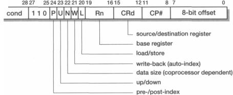
5.18Coprocessor data transfers
The coprocessor data transfer instructions are similar to the immediate offset forms of the word and unsigned byte data transfer instructions described earlier, but with the offset limited to eight bits rather than 12.
Auto-indexed forms are available, with preand post-indexed addressing.
Binary encoding
31
Figure 5.16 Coprocessor data transfer instruction binary encoding.
Description
Assembler format
The instruction is offered to any coprocessors which may be present; if none accepts it ARM takes the undefined instruction trap and may use software to emulate the coprocessor. Normally the coprocessor with coprocessor number CP#, if present, will accept the instruction.
The address calculation takes place within the ARM, using an ARM base register (Rn) and an 8-bit immediate offset which is scaled to a word offset by shifting it left two bit positions. The addressing mode and auto-indexing are controlled in the same way as the ARM word and unsigned byte transfer instructions. This defines the first transfer address; subsequent words are transferred to or from incrementing word addresses.
The data is supplied by or received into a coprocessor register (CRd), with the number of words transferred being controlled by the coprocessor and the N bit selecting one of two possible lengths.
The pre-indexed form:
LDCISTC{<cond>}{L} <CP#>, CRd, [Rn, <offset>]
{ ! } The post-indexed form:
LDCISTC{<cond>}{L} <CP#>, CRd, |
[Rn], |
<offset> |
Coprocessor register transfers |
139 |
In both cases LDC selects a load from memory into the coprocessor register, STC selects a store from the coprocessor register into memory. The L flag, if present, selects the long data type (N= 1). <of fset> is # + /-<8-bit immediate;-.
Examples
Notes
LDC |
p6, |
CO, |
[r1] |
|
STCEQL |
p5, |
Cl, |
[ r 0 ] , |
#4 |
1.The interpretation of the N and CRd fields is coprocessor-dependent. The use shown above is recommended and will maximize compatibility with ARM devel opment tools.
2.If the address is not word-aligned the two least significant bits will be ignored, though some ARM systems may raise an exception.
3.The number of words transferred is controlled by the coprocessor and the ARM will continue to generate sequential addresses until the coprocessor indicates that the transfer should complete (see 'Data transfers' on page 102). During the data transfer the ARM will not respond to interrupt requests, so coprocessor designers should be careful not to compromise the system interrupt response time by allow ing very long data transfers.
Limiting the maximum transfer length to 16 words will ensure that coprocessor data transfers take no longer than worst-case load and store multiple register instructions.
5.19Coprocessor register transfers
These instructions allow an integer generated in a coprocessor to be transferred directly into a ARM register or the ARM condition code flags. Typical uses are:
•A floating-point FIX operation which returns the integer to an ARM register;
•A floating-point comparison which returns the result of the comparison directly to the ARM condition code flags where it can determine the control flow;
•A FLOAT operation which takes an integer value from an ARM register and sends it to the coprocessor where it is converted to floating-point representation and placed in a coprocessor register.
The system control coprocessors used to control the cache and memory management functions on the more complex ARM CPUs (Central Processing Units) generally use these instructions to access and modify the on-chip control registers.