

Chen Y.Resonant gate drive techniques for power MOSFETs
.pdfMany loss factors contribute to VRM efficiency drop at high frequencies, such as power MOSFET gate drive loss, switching loss, magnetic core loss, and conduction loss. When the switching frequency of a VRM goes higher, all these losses surge rapidly, resulting in a lower efficiency. However, while all above loss factors are involved in degrading the overall efficiency of a VRM, the contribution of each loss factor differs. Recognizing the impossibility to reduce all these losses, it is necessary to identify those major loss factors so that proper research efforts can be focused to improve VRM efficiency at high frequencies.
To evaluate the contribution of MOSFET gate drive loss in overall efficiency drop, one experiment was carried out [I-7]. In this experiment, a typical single channel Synchronous Rectifier Buck converter was built, using TPS1111N (made by Texas Instruments) as power MOSFETs and HIP2100 (made by Harris Corporation, now Intersil Corporation) as the gate driver. The converter was designed with an input voltage at 3.3 Volts, an output voltage at 1.2 Volts, a full load at 8 Amps, and a switching frequency at 2 MHz. Its circuit diagram is also drawn in Figure 1.5. By calculating the efficiency difference between η (the overall efficiency of the converter) and η’ (the converter efficiency when MOSFET gate drive loss is excluded from the calculation), the contribution of gate drive loss can be evaluated.
TPS1111N
|
|
|
|
|
|
|
|
|
|
|
|
|
|
|
|
|
|
|
|
|
|
|
|
|
|
|
|
|
|
|
|
|
|
|
|
|
|
|
|
|
|
|
|
|
|
|
|
|
|
|
|
|
|
|
|
|
|
|
|
|
|
|
|
|
|
|
|
|
|
|
|
|
|
|
|
|
|
|
|
V i n |
|
|
|
|
|
|
|
|
|
|
|
|
|
|
|
|
|
|
|
L=150nH |
|||
|
|
|
|
|
|
|
|
|
|
|
|
|
|
|
|
|
|
|
|
|
|||||
|
|
|
|
|
|
|
|
|
|
|
|
|
|||||||||||||
|
|
|
|
|
|
|
|
|
|
|
|
|
|
|
|
|
|
|
|
|
|
|
|
|
|
|
|
|
|
|
|
|
|
|
|
|
|
|
|
|
|
|
|
|
|
|
|
|
|
|
|
|
|
|
|
|
|
|
|
|
|
|
|
|
|
|
|
|
|
|
|
|
|
|
|
||
|
|
|
|
|
|
|
|
|
|
|
|
|
|
|
|
|
|
|
|
|
|
|
|
||
|
|
|
HIP2100 |
|
|
|
|
|
|
|
|
|
|
|
|
||||||||||
|
|
|
|
|
|
|
|
|
|
|
C=60μF |
||||||||||||||
|
|
|
|
|
|
|
|
|
|
|
|
|
|
|
|
|
|
|
|
|
|
||||
|
|
|
|
|
|
|
|
|
|
|
|
|
|
|
|
|
|
|
|
|
|
|
|
|
|
|
|
|
|
|
|
|
|
|
|
|
|
|
|
|
|
|
|
|
|||||||
|
|
|
|
|
|
|
|
|
|
|
|
|
|
|
|
|
|
TPS1111N |
|||||||
|
|
|
|
|
|
|
|
|
|
|
|
|
|
|
|
|
|
||||||||
|
|
Figure 1.5 A Synchronous Rectifier Buck Converter [I-7] |
|||||||||||||||||||||||
As can be seen from the measured efficiency in Figure 1.6, the overall efficiency η peaks at 78% at about half load (load current Io=4A) and drops to 52% at light load (Io=0.5A).
5
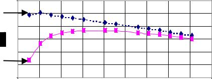
By excluding the gate drive loss from efficiency calculation, a dotted curve η’ is also plotted in Figure 1.6. The difference between η and η’ shows that power MOSFET gate drive loss causes about 5% efficiency drop at full load and more than 35% drop at light load. Although these numbers may vary when the circuit in Figure 1.5 is implemented with different components, they demonstrate the significance of MOSFET gate drive loss in causing VRM efficiency drop.
100 η’ 90
80 |
70 |
60 |
η
50
40
0 |
1 |
2 |
3 |
4 |
5 |
6 |
7 |
8 |
9 |
Io (A)
Figure 1.6 Efficiency of the Converter in Figure 1.5 [I-7]
By knowing the significance of MOSFET gate drive loss, much valuable research has been conducted in recent years. It is now a common understanding that the power loss in driving a MOSFET can expressed as [I-8]:
P |
= C |
in |
×V 2 |
× f |
(1.1) |
gd |
|
gate |
|
|
in which Pgd is MOSFET gate drive loss, Cin is the equivalent input capacitance of the MOSFET, Vgate is the voltage level of the power supply to the gate drive circuitry, and f is the switching frequency that the MOSFET is working at. Since Pgd is proportional to the switching frequency, Equation 1.1 explains the significance of gate drive loss at high frequencies.
Presenting the basic understanding to the MOSFET gate drive loss issue, Equation 1.1 gives the starting point, not the end, of solving the gate drive problem. The ultimate goal of solving the problem is to find an effective way to reduce power MOSFET gate drive loss, so that a VRM can be working at high frequencies even with an adequately high efficiency. This goal is essentially the purpose of this thesis: to investigate resonant gate
6
drive techniques so that the power MOSFET gate drive loss can be effectively reduced. More specifically, this thesis is to explain the fundamental loss mechanism in a power
MOSFET gate driver, investigate the |
possibility |
in reducing |
this |
loss by |
employing |
resonant power conversion techniques, |
and finally |
propose a |
simple |
circuit |
that serves |
this purpose. By reducing MOSFET gate drive loss, this thesis is expected to help improve the performance of any system built upon power MOSFETs, including almost all high frequency switching-mode power supplies, such as VRMs.
1.2 Thesis Organization
This thesis is divided into seven chapters. The content of each chapter is outlined below.
Chapter I, “Introduction,” introduces the wide use of power MOSFETs in power electronics. In many applications such as the VRM, reducing MOSFET gate drive is critical in improving system efficiency. The purpose of this thesis is to investigate resonant gate drive techniques so that the gate drive loss can be effectively reduced.
Chapter II, “Loss Analysis of Conventional Gate Drivers,” analyzes the fundamental loss mechanisms in conventional “Totem-Pole” gate drive circuits. Simplifying the driver into a R-C first-order system, Chapter II explains the power loss involved in driving a power MOSFET. Very interestingly, it is also found that no matter large or small the value of the gate resistance is, it does not change gate drive loss. This chapter is finally concluded with a discussion of some other possible losses in driving a MOSFET.
Chapter III is titled as “Resonant Gate Drive Techniques.” By adding a reactive component in the simplified circuit in Chapter II, MOSFET gate drive loss can be reduced and there arises the origin of resonant gate drive techniques. Chapter III analyzes the energy distribution in a R-L-C second-order system and introduces a new resonant gate driver.
7
Chapter IV, “A New Resonant Gate Driver,” describes the basic operation of the new resonant gate drive circuit, to reveal the fact that this new driver features complete energy recovery during both charging and discharging transitions. Also, with the use of this new driver, the cross-conduction loss in a conventional driver is eliminated. Hence the gate drive loss in the proposed circuit is much lower than that in a conventional gate driver. All these analysis are finally verified by simulation and experiment results.
Chapter V, “Comparison between Different Gate Drivers,” proves the advantages of the proposed driver over other gate drivers. It includes the following sections:
∙loss comparison between a conventional gate driver and the proposed driver;
∙efficiency improvement of a Push-Pull Forward Converter; and
∙comparison with other existing resonant gate drivers.
Chapter VI is titled as “Half-Bridge MOSFET Gate Drive with Coupled Resonance.” To further expand the use of the resonant drive circuit in Chapter IV, Chapter VI proposes another circuit to drive two power MOSFETs in any type of Half-Bridge configurations. Compared with conventional Half-Bridge gate drivers, this circuit in Chapter VI possesses two pronounced advantages. First, it can eliminate the Bootstrap loss in conventional drivers. Second, it takes advantages of the circuit in Chapter IV so that the gate drive loss of each MOSFET is also greatly reduced. Also, the circuit in Chapter VI is immune to leakage inductance problems.
Chapter VII, “Conclusion,” concludes the whole thesis with an expectation of the use the resonant gate drive techniques for IGBTs.
8
References:
[I-1] B. K. Bose (Editor), Modern Power Electronics, IEEE Press, Piscataway, NJ, 1992, pp. 3-39
[I-2] IEEE PELS homepage, http://www.pels.org
[I-3] N. Mohan, T. M. Undeland, and W. P. Robbins, Power Electronics: Converters, Applications, and Design, Second Edition, John Wiley & Sons, Inc., 1995
[I-4] B. K. Bose (Editor), Modern Power Electronics, IEEE Press, Piscataway, NJ, 1992, pp. ix-x
[I-5] Xunwei Zhou, Low-Voltage, High-Efficiency, Fast-Transient Voltage Regulator Module, Ph. D. Dissertation, Virginia Polytechnic Institute and State University, 1999
[I-6] William Stallings, Computer Organization and Architecture: Design for Performance, Fifth Edition, Prentice Hall, 1996
[I-7] Virginia Power Electronics Center (VPEC), Investigation of Power Management Issues for Next Generation microprocessors, Quarterly Progress Reports to VRM Consortium
[I-8] Dragan Maksimovic, “A MOS Gate Drive with Resonant Transitions,” IEEE
PESC (Power Electronics Specialists Conference) Proceeding, 1991, pp. 527-532
9
Chapter II
Loss Analysis of Conventional Gate Drive Circuits
As stated in Chapter I, the purpose of this thesis is to reduce the loss in driving a power MOSFET. This issue of MOSFET gate drive loss can be further split into following two questions:
1)where does gate drive loss come from?
2)how does one reduce above loss effectively?
This chapter is to answer the first question. By analyzing presently used gate drivers, this chapter explains the loss mechanism in driving a power MOSFET, locates all power losses involved, and consequently offers necessary preparations for answering the second question in later chapters.
2.1 Conventional Gate Drivers
In today’s power IC (Integrated Circuit) market, there are various kinds of power MOSFET gate drive chips available. Most of them come from semiconductor companies such as Intersil Corporation (formerly Harris), Texas Instruments, Micrel Semiconductor, and International Rectifiers. Usually all these commercial gate drivers have the same circuit configuration: a “Totem-Pole” structure, in which the drain terminal of a P- channel MOSFET is connected to the drain of an N-channel MOSFET. In this thesis, all gate drivers with above simple “Totem-Pole” structure are referred to as “conventional gate drivers.” Figure 2.1 shows the circuit diagram of a conventional gate driver, along with the power MOSFET being driven.
In the left block labeled with “Gate Driver” in Figure 2.1, Q1 is a P-channel MOSFET
and Q2 is an N-channel MOSFET. They are connected at their drains and form the aforementioned “Totem-Pole” structure. The two diodes anti paralleled with Q1 and Q2 are their internal body diodes. In this circuit diagram, the “Gate Driver” block has four
10

terminals. One of them is connected to a DC voltage source Vgate, one is pulled down to the ground, the third terminal receives a control signal Vtrig from a PWM (Pulse Width Modulation) controller, and the last terminal goes to the gate of the power MOSFET in the right block. Also notice that in this circuit diagram, the gates of Q1 and Q2 are tied together to achieve fast driving capability [II-1].
Vgate |
|
|
|
|
|
|
Vd |
Q1 |
Rg |
Vg |
|
Vtrig |
|
||
Q2 |
|
|
|
|
|
|
Cin |
Gate Driver |
|
Power MOSFET |
|
|
|
||
Figure 2.1 |
Circuit Diagram of Conventional Gate Drivers |
||
Also in Figure 2.1, the resistor Rg between “Gate Driver” and “Power MOSFET” stands for the gate resistance of the power MOSFET. It includes the MOSFET semiconductor bulk resistance [II-2], power packaging resistance, and the on-resistance of Q1 and Q2. In some applications, an external resistor can be seen in series with the gate of the power MOSFET to prevent high frequency rings; in those applications, Rg also includes the external resistor.
In the right block labeled with “Power MOSFET”, Cin stands for the equivalent gate input capacitance of the power MOSFET. It is not external to the MOSFET, although it is drawn so for convenience. Because of “Miller Effect” [II-3], the gate capacitance of a power MOSFET actually varies at different voltage levels. In other words, Cin is nonlinear in reality. Above Cin can thus be regarded as the average capacitance over the complete charging and discharging transitions. Figure 2.2 shows the relationship between the gate voltage and the gate charge of a typical power MOSFET. The flat
11

portion in the curve comes from the “Miller Effect.” If the final voltage applied at the gate is Vgate, then Cin can be defined as
Qgate
Cin = (2.1)
Vgate
Already shown in Equation 1.1, Cin is used commonly in calculating gate drive losses, although, important enough to emphasize again, Cin is a nonlinear capacitor.
Vg |
|
|
Vgate |
|
|
0 |
Qgate |
Qg |
|
||
Figure 2.2 |
Relationship between Gate Charge and Gate Voltage |
|
2.2 Equivalent Circuits
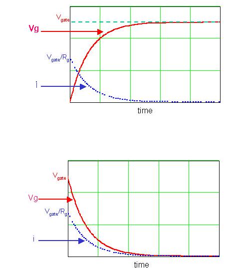
With the circuit diagram in Figure 2.1, the operation of conventional gate drivers can be explained as follows: when the control signal commands the gate driver to turn on the power MOSFET, Vtrig put a negative signal (logically low) at the gates of both Q1 and Q2. Since Q1 is a P-channel MOSFET and Q2 is of N-channel, Q1 will be turned on and Q2 will be off. A current will then flow out of the voltage source Vgate, through Q1 and Rg, into the gate capacitor Cin. This current flow will not stop until the voltage across Cin reaches Vgate. During this transition (more often referred as “charging period”), the whole circuit in Figure 2.1 works the same as the simplistic circuit drawn in Figure 2.3a.
Similar is the other transition: when the control signal commands the gate driver to turn off the power MOSFET, Vtrig puts a positive signal (logically high) at the gates of Q1 and Q2 and consequently Q1 will be turned off and Q2 will be on. A current will then flow out of Cin, through Rg and Q2, and return back from the ground. This current flow will
12

not stop until Vg goes to zero. During this transition (more often referred as “discharging period”), the whole circuit in Figure 2.1 works exactly the same as the simplistic circuit draw in Figure 2.3b.
|
Rg |
|
+ |
Rg |
+ |
|
i |
|
i |
||
Vgate |
|
|
|
||
|
Cin |
Vg |
|
Vg |
|
|
|
|
Cin |
||
|
|
|
_ |
|
_ |
|
(a) |
|
|
|
(b) |
Figure 2.3 Equivalent Circuits of Conventional Gate Drive Circuits:
(a) during charging period, and (b) During discharging period [II-4]
Since the circuits in Figure 2.3 are much simpler than the original circuit in Figure 2.1 but can perform the same functions, they will be used as equivalent circuits in analyzing the power loss involved in MOSFET gate drive.
The equivalent circuits in Figure 2.3 indicate that during both charging and discharging periods, a conventional gate driver works exactly as a simple R-C first-order system. The only differences between charging and discharging are the initial voltage level across Cin and the involvement of the voltage source Vgate. During the charging period, the initial value of Vg is zero and Vgate is involved; during the discharging period, Vg is initially Vgate and the voltage source is not involved. Also with the help of equivalent circuits, more detailed waveforms can be derived. During the charging period, like any R-C firstorder system, the voltage Vg in Figure 2.3a rises exponentially while the current i decays exponentially. Their waveforms are shown in Figure 2.4 (the reference direction of Vg and i are defined in Figure 2.3a). During the discharging period, both Vg and i decay exponentially and their waveforms are shown in Figure 2.5 (the reference direction of Vg and i are defined in Figure 2.3b). Again, given that Cin is nonlinear in reality, actual waveforms in Figure 2.1 may not be exactly the same as Figures 2.4 and 2.5, but with minor difference. Actual waveforms will be described in next section.
13
Moreover, the time constant of all four exponential waveforms in Figure 2.4 and 2.5 can be expressed as follows:
t = |
|
1 |
(2.2) |
|
Rg |
×Cin |
|||
|
|
Since a R-C first-order system needs 3τ to 5τ time to reach its steady state after a step stimulus, Equation 2.2 can be used to estimate the driving speed of a conventional gate driver. Driving speed is always a very important parameter to evaluate the performance of gate drivers, especially at high frequencies.
Figure 2.4 Current and Voltage Waveforms at Charging Period
Figure 2.5 Current and Voltage Waveforms at Discharging Period
14