

09.RF power amplifiers
.pdf178 RF POWER AMPLIFIERS
is supplied through a resistor and max D 50% when the bias to the collector is supplied through an RF choke.
9.3THE CLASS C AMPLIFIER
The class C amplifier is useful for providing a high-power continuous wave (CW) or frequency modulation (FM) output. When it is used in amplitude modulation schemes, the output variation is done by varying the bias supply. There are several characteristics that distinguish the class C amplifier from the class A or B amplifiers. First of all it is biased so that the transistor conduction angle is <180°. Consequently the class C amplifier is clearly nonlinear in that it does not directly replicate the input signal like the class A and B amplifiers do (at least in principle). The class A amplifier requires one transistor, the class B amplifier requires two transistors, and the class C amplifier uses one transistor. Topologically it looks similar to the class A except for the dc bias levels. It was noted that in the class B amplifier, an output filter is used optionally to help clean up the output signal. In the class C amplifier, such a tuned output is necessary in order to recover the sine wave. Finally, class C operation is capable of higher efficiency than either of the previous two classes, so for the appropriate signal types they become very attractive as power amplifiers.
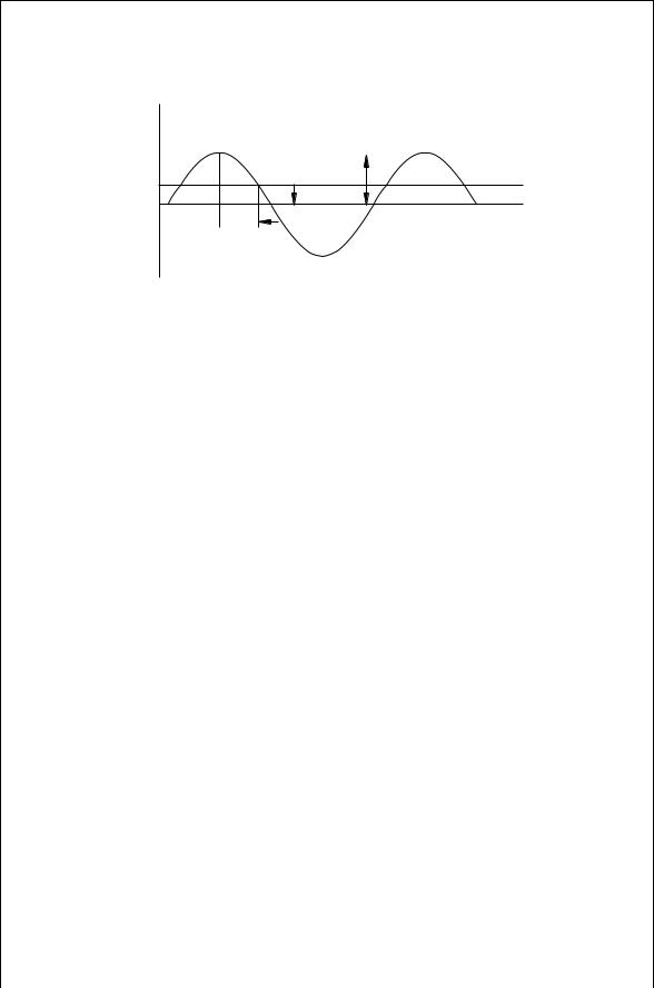
The class C amplifier shown in Fig. 9.9 gives the output circuit for a power bipolar transistor (BJT) with the required tuned circuit. An N-channel enhance- ment-mode metal oxide semiconductor field effect transistor (MOSFET) can be used in place of the BJT. The Q of the tuned circuit will determine the bandwidth of the amplifier. The large inductance RF coil in the collector voltage supply ensures that only dc current flows there. During that part of the input cycle when the transistor is on, the bias supply current flows through the transistor and the output voltage is approximately 90% of VCC. When the transistor is off, the supply current flows into the blocking capacitor. The current waveform at the
|
|
|
+ |
Vcc |
|
|
|
– |
|
|
|
|
RFC |
|
|
R G |
C B |
C B |
|
|
|
|
||
|
+ |
RFC |
C o |
R L |
VGsinωt |
|
|
L o |
|
– |
|
+ |
|
|
|
Vbb |
|
|
|
|
|
– |
|
|
|
|
|
|
FIGURE 9.9 A simple class C amplifier where VBB determines the conduction angle.
THE CLASS C AMPLIFIER |
179 |
ic
|
|
idc |
IC |
ψ 
FIGURE 9.10 The collector current waveform for class C operation.
collector can be modeled as the waveform shown in Fig. 9.10:
iC ωt |
D |
|
IC |
|
IOC sin ωt , ωt C |
9.35 |
|
0, |
otherwise |
|
For class C operation, the magnitude of the quiescent current is jICj < IOC. The point where quiescent current equals the total current is
iC |
32 |
š |
D 0 D IC IOC sin |
32 |
š |
|
||
|
|
|
|
|
|
|
||
|
|
|
|
0 D IC C IOC cos |
|
|
|
9.36 |
This determines the value of the quiescent current in terms of the conduction angle 2 :
IC D IOC cos |
9.37 |
The dc current from the power supply is the average of the total collector current iC " :
|
1 |
0 |
2 |
|
|
|
Idc D |
iC " d " |
|
||||
|
|
|
||||
2 |
|
|||||
D |
|
|
|
3/2 |
IC IOC sin " d " |
|
2 3/2 C |
|
|||||
|
1 |
|
|
|
|
|
D |
1 |
|
IC C IOC sin |
9.38 |
||
|
||||||
|
||||||

180 RF POWER AMPLIFIERS
Evaluation of the integral makes use of the trigonometric identity, cos ˛ š ˇ D cos ˛ cos ˇ Ý sin ˛ sin ˇ. From Eq. (9.36) the dc current is
IOC |
sin |
cos |
9.39 |
Idc D |
This gives the dc current from the power supply in terms of IOC and the conduction angle , so power supplied by the source is
Pin D VCCIdc |
9.40 |
The ac component of the current flows through the blocking capacitor and into the load. Harmonic current components are shorted to ground by the tuned circuit. The magnitude of the output voltage at the fundamental frequency is found using the Fourier method:
1 |
2 |
|
|
|
|
|
|
|
|
|
|
|
|
|
|
|
|
||||
0 |
|
|
|
|
|
|
|
|
|
|
|
|
|
|
|
|
|||||
VO O D |
|
|
iC " RL sin "d " |
|
|
|
|
|
|
|
|
|
|||||||||
|
|
|
|
|
|
|
|
|
|
||||||||||||
|
|
|
|
3/2 |
IC IOC sin " sin "d " |
|
|
|
|
|
|||||||||||
D L 3/2 C |
|
|
|
|
|
||||||||||||||||
|
|
R |
|
|
|
|
|
|
|
|
|
|
|
|
|
|
|
|
|
|
|
|
RL |
2IC |
|
|
cos " |
|
3/2 C |
C |
IOC |
" |
|
sin 2" |
|
3/2 C |
|
||||||
|
|
|
|
2 |
2 |
|
|
||||||||||||||
D |
|
|
|
|
|
|
|
|
|
|
|
||||||||||
|
|
|
|
|
|
|
|
3/2 |
|
|
|
|
|
3/2 |
|
|
|||||
|
|
|
|
|
|
|
|
|
|
|
|
|
|
|
|
||||||
|
|
|
|
|
|
|
|
|
|
|
|
|
|
|
|
|
|
|
|
|
|
|
|
|
|
|
|
|
|
|
|
|
|
|
|
|
|
|
|
|
|
|
|
9.41
9.42
D |
2IC sin |
C |
O2 |
2 |
2 |
[sin 3 C 2 sin 3 2 ] |
|
||
|
RL |
|
|
|
|
1 |
|
|
|
|
|
|
IC |
|
|
|
|
||
9.43 The quiescent current term, IC, is replaced by Eq. (9.37) again, and the trigonometric identity for sin ˛ cos ˇ is used:
VO O D |
O |
sin 2 C |
|
4 |
sin 2 sin 2 |
9.44 |
||
|
RLIC |
|
|
|
1 |
|
|
|
VO O D |
RLIOC |
2 sin 2 |
|
|
|
|
|
9.45 |
2 |
|
|
|
|
||||
The ac output power delivered to the load is |
|
|
||||||
|
|
PO D |
VO O2 |
|
9.46 |
|||
|
|
2RL |
|
|
||||
The efficiency (neglecting the input power) is simply the ratio of the output ac power to the input dc power. The maximum output power occurs when VO O D
THE CLASS C AMPLIFIER |
181 |
VCC. The maximum efficiency is then [2]
max D |
Pdc |
D |
2RL |
VCCIdc |
9.47 |
||
|
POmax |
|
VCC2 |
1 |
|
|
|
D |
2 |
sin 2 |
|
|
|
9.48 |
|
4 sin |
|
|
|
|
|||
|
cos |
|
|
|
|||
|
|
|
|
|
|
|
|
A plot of this expression (Fig. 9.11) clearly illustrates the efficiency in terms of the conduction angle for class A, B, and C amplifiers. The increased efficiency of the class C amplifier is a result of the collector current flowing for less than a half-cycle. When the collector current is maximum, the collector voltage is minimum, so the power dissipation is inherently lower than class B or class A operation.
Another important parameter for the power amplifier is the ratio of the maximum average output power where VO O D VCC, to the peak instantaneous output power:
Maximum Efficiency
|
|
|
|
|
|
|
|
|
r D |
|
POmax |
|
|
|
|
|
|
9.49 |
|||||
|
|
|
|
|
|
|
|
|
VCmaxiCmax |
|
|
|
|
|
|
||||||||
100.0 |
|
|
|
|
|
|
|
|
|
|
|
|
|
|
|
|
|
|
|
|
|
|
|
|
|
|
|
|
|
|
|
|
|
|
|
|
|
|
|
|
|
|
|
|
|
|
|
90.0 |
|
|
|
|
|
|
|
|
|
|
|
|
|
|
|
|
|
|
|
|
|
|
|
|
|
|
|
|
|
|
|
|
|
|
|
|
|
|
|
|
|
|
|
|
|
|
|
|
|
|
|
|
|
|
|
|
|
|
|
|
|
|
|
|
|
|
|
|
|
|
|
80.0 |
|
|
|
|
|
|
|
|
|
|
|
|
|
|
|
|
|
|
|
|
|
|
|
|
|
|
|
|
|
|
|
|
|
|
|
|
|
|
|
|
|
|
|
|
|
|
|
|
|
|
|
|
|
|
|
|
|
|
|
|
|
|
|
|
|
|
|
|
|
|
|
70.0 |
|
|
|
|
|
|
|
|
|
|
|
|
|
|
|
|
|
|
|
|
|
|
|
|
|
|
|
|
|
|
|
|
|
|
|
|
|
|
|
|
|
|
|
|
|
|
|
|
|
|
|
|
|
|
|
|
|
|
|
|
|
|
|
|
|
|
|
|
|
|
|
60.0 |
|
|
|
|
|
|
|
|
|
|
|
|
|
|
|
|
|
|
|
|
|
|
|
|
|
|
|
|
|
|
|
|
|
|
|
|
|
|
|
|
|
|
|
|
|
|
|
|
|
|
|
|
|
|
|
|
|
|
|
|
|
|
|
|
|
|
|
|
|
|
|
|
|
|
|
|
|
|
|
|
|
|
|
|
|
|
|
|
|
|
|
|
|
|
|
|
Class |
|
|
C |
|
|
|
|
B |
|
|
AB |
|
|
|
|
|
|
|||||
50.0 |
|
|
|
|
|
|
|
|
|
|
|
|
|
|
|
|
|
|
|
|
|
|
|
|
|
|
|
45 |
90 |
135 |
180 |
225 |
270 |
315 |
360 |
||||||||||||
0 |
|
|
|
||||||||||||||||||||
Conduction Angle
FIGURE 9.11 Power efficiency for class A, B, and C amplifiers.

182 RF POWER AMPLIFIERS
The maximum average output power occurs when VO O D VCC and is given by
|
V2 |
|
|
|||
POmax D |
CC |
|
|
9.50 |
||
2RL |
|
|||||
D |
IOC2 RL2 |
|
2 |
sin 2 2 |
9.51 |
|
4 2 |
|
2RL |
||||
|
|
|
||||
The maximum voltage at the collector is the output voltage ac voltage swing plus the bias voltage:
VCmax D 2VCC D |
IOCRL |
2 sin 2 |
9.52 |
2 |
|||
The maximum current is |
|
|
|
iCmax D IC C IOC D IOC cos C IOC. |
9.53 |
||
The ratio of the maximum average power to the peak power from (9.49) is [2]
r |
D |
2 sin 2 |
|
9.54 |
||
|
|
|||||
|
8 1 |
|
cos |
|
||
|
|
|
|
|
|
|
A plot of this ratio as a function of conduction angle in Fig. 9.12 shows that maximum efficiency of the class C amplifier occurs when there is no output
Power Ratio, r
0.150
0.125
0.100
0.075
0.050
Class |
C |
B |
AB |
0.025
0.000
0 |
45 |
90 |
135 |
180 |
225 |
270 |
315 |
360 |
Conduction Angle
FIGURE 9.12 Maximum output power to the peak power ratio.

CLASS C INPUT BIAS VOLTAGE |
183 |
power. Nevertheless, Figs. 9.11 and 9.12 indicate the trade-offs in choosing the appropriate conduction angle for class C operation.
9.4CLASS C INPUT BIAS VOLTAGE
Device SPICE models for RF power transistors are relatively rare. Manufacturers often do supply optimum generator and load impedances that have been found to provide the rated output power for the designated frequency. The circuit shown in Fig. 9.9 is a generic example of a 900 MHz amplifier with a bandwidth of 18 MHz in which the manufacturer has determined empirically the optimum ZG and ZL. The Q of the output tuned circuit then is
f0 |
9.55 |
Q D f |
The Q determines the inductance and capacitance of the output resonant circuit:
C D |
Q |
9.56 |
|
ω0RL |
|||
L D |
RL |
9.57 |
|
ω0Q |
|
||
Furthermore, if the desired output power is POmax, the collector voltage source, VCC, and the maximum collector current is icmax, then the average to peak power ratio, r, is found from Eqs. (9.49) and (9.54). Iterative solution of Eq. (9.54) gives the value for the conduction angle, . This will then allow for estimation of the maximum efficiency from Eq. (9.48). Alternatively, for a given desired efficiency, the conduction angle, , can be obtained by iterative solution of Eq. (9.48). Numerically it is useful to take the natural logarithm of Eq. (9.48) before searching iteratively for a solution:
ln max D ln 2 sin 2 ln[4 sin cos ] |
9.58 |
The efficiency expression can be modified to account for the non zero saturation collector–emitter voltage.
|
max D |
4 sin |
cos |
VCC |
|
|
|
|
2 |
sin 2 |
|
VCC Vsat |
9.59 |
|
|
|
|
|||
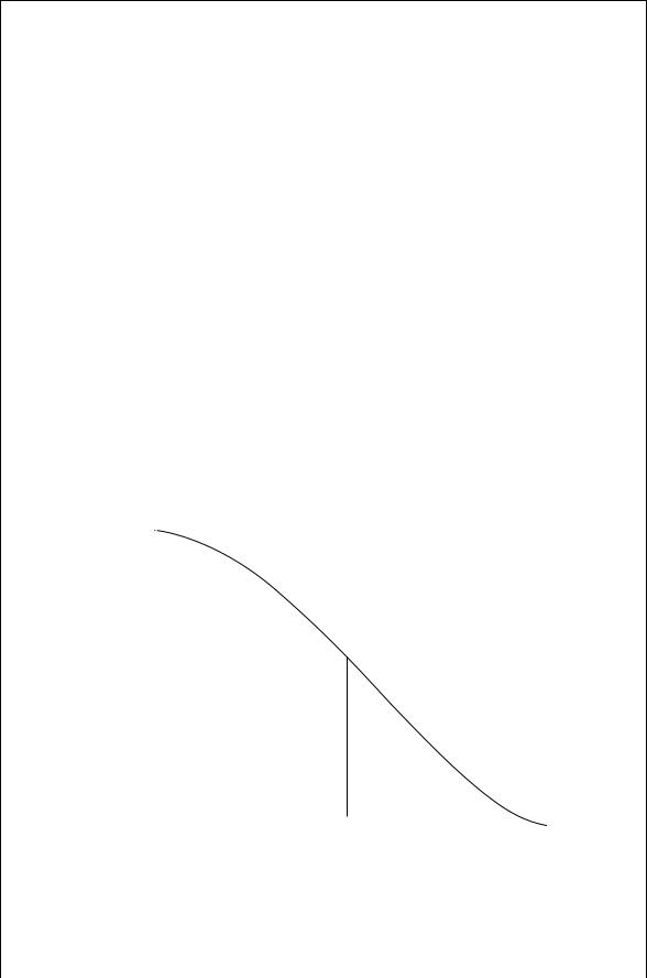
To achieve the desired conduction angle, the emitter–base junction must be biased so that the transistor will be in conduction for the desired portion of the input signal. Collector current flows when VBE > 0.7. First it is necessary to determine the required generator voltage amplitude, VO G, that will produce the desired maximum output current. This is illustrated in Fig. 9.13 where the input ac signal
184 RF POWER AMPLIFIERS
|
|
|
V BE –V BB |
V G |
|
|
|
|
ψ 
FIGURE 9.13 Conduction angle dependence on VBB.
is superimposed on the emitter bias voltage. The input voltage commences to rise above the turn on voltage of the transistor at
VO BB D VBE VO G cos |
9.60 |
In this way the base bias voltage is determined.
9.5THE CLASS D POWER AMPLIFIER
Inspection of the efficiency and output power of a class C amplifier reveals that 100% efficiency only occurs when the output power is zero. A modification of class B operation shown in [3] indicates that judicious choice of bias voltages and circuit impedances provide a clipped voltage waveform at the collector of the BJT while, in the optimum case, retaining the half sine wave collector current. In the limit the clipped waveform becomes a square wave. This is no longer linear, and thus is distinguished from the class B amplifier.
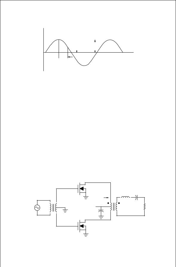
The class D amplifier shown in Fig. 9.14 superficially looks like a class B amplifier except for the input side bias. In class D operation the transistors act as
|
|
M 1 |
L |
C |
|
|
|
||
|
|
|
R L |
|
v |
|
+ |
|
R 'L |
in |
V |
CC |
||
|
– |
|
||
|
|
|
|
1 : n Filter
M 2
FIGURE 9.14 Class D power amplifier.
THE CLASS F POWER AMPLIFIER |
185 |
near ideal switches that are on half of the time and off half of the time. The input ideally is excited by a square wave. If the transistor switching time is near zero, then the maximum drain current flows while the drain–source voltage, VDS D 0. As a result 100% efficiency is theoretically possible. In practice the switching speed of a bipolar transistor is not sufficiently fast for square waves above a few MHz, and the switching speed for field effect transistors is not adequate for frequencies above a few tens of MHz.
9.6THE CLASS F POWER AMPLIFIER
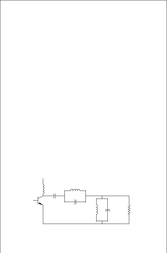
“A class F amplifier is characterized by a load network that has resonances at one or more harmonic frequencies as well as at the carrier frequency” [2, p. 454]. The class F amplifier was one of the early methods used to increase amplifier efficiency and has attracted some renewed interest recently. The circuit shown in Fig. 9.15 is a third harmonic peaking amplifier where the shunt resonator is resonant at the fundamental and the series resonator at the third harmonic. More details on this and higher-order resonator class F amplifiers are found in [4]. When the transistor is excited by a sinusoidal source, it is on for approximately half the time and off for half the time. The resulting output current waveform is converted back to a sine wave by the resonator, L1, C1. The L3, C3 resonator is not quite transparent to the fundamental frequency, but blocks the third harmonic energy from getting to the load. The drain or collector voltage, it would seem, will range from 0 to twice the power supply voltage with an average value of VCC. The third harmonic voltage on the drain or collector, if it has the appropriate amplitude and phase, will tend to make this device voltage more square in shape. This will make the transistor act more like a switch with the attendant high efficiency. It is found that maximum “squareness” is achieved if the third harmonic voltage is 1/9th of the fundamental voltage. This will give a maximum collector efficiency of 88.4% [2, pp. 454–456].
 VCC
VCC
L 3
C B
C 3 |
|
R L |
L 1 |
C 1 |
FIGURE 9.15 Class F third harmonic peaking power amplifier.

186 RF POWER AMPLIFIERS
The Fourier expansion of a square wave with amplitude from C1 to 1 and period 2 is
4 sin 3x sin 5x sin x C C C Ð Ð Ð
3 5
Consequently, to produce a square wave voltage waveform at the transistor terminal, the load must be a short at even harmonics and large at odd harmonics. Ordinarily only the fundamental second harmonic and third harmonic impedances are determined. In the typical class F amplifier shown in Fig. 9.15, the L1C1 tank circuit is resonant at the output frequency, f0, and the L3C3 tank circuit is resonant at 3f0. It has been pointed out [5] that the blocking capacitor, CB, could be used to provide a short to ground at 2f0 rather than simply acting as a dc block.
The design of the class F amplifier final stage proceeds by first determining C1 from the desired amplifier bandwidth. The circuit Q is assumed to be determined solely by the L1, C1, and RL. Thus
Q D ω0C1RL D |
ω0 |
|
||
ω |
|
|||
or |
|
|||
1 |
|
|
9.61 |
|
C1 D |
|
|
||
RL ω |
||||
Once C1 is determined, the inductance must be that which resonates the tank at f0:
1 |
9.62 |
L1 D ω02C1 |
At 2f0 the L1C1 tank circuit has negative reactance, and the L3C3 tank circuit has positive reactance. The capacitances CB and C3 can be set to provide a short to ground:
1 |
|
2ω0L3 |
|
2ω0L1 |
D 0 |
9.63 |
|
|
|
C |
|
C |
|
||
2ω0CB |
1 2ω0 2L3C3 |
1 2ω0 2L1C1 |
|||||
On multiplying through Eq. (9.63) by ω0 and recognizing that L3C3 D 1/9ω02, L1C1 D 1/ω02, this equation reduces to
1 |
|
|
|
2/ 9C3 |
|
|
2/C1 |
|||||
0 D |
|
|
C |
|
|
|
C |
|
|
|||
CB |
1 4/9 |
1 4 |
||||||||||
or |
4 |
|
|
4 |
|
|
|
|||||
1 |
|
|
|
|
9.64 |
|||||||
|
|
|
D |
|
|
|
|
|||||
|
CB |
5C3 |
3C1 |
|||||||||
which is the requirement for series resonance at 2f0. In addition, at the fundamental frequency, CB and the L3C3 tank circuit can be tuned to provide no
THE CLASS F POWER AMPLIFIER |
187 |
reactance between the transistor and the load, RL. This eliminates the approximation that the L3C3 has zero reactance at the fundamental:
1 |
|
ω0L3 |
9.65 |
|
0 D |
|
C |
|
|
ω0CB |
1 ω02L3C3 |
|||
CB D 8C3 |
|
|
9.66 |
|
This value for CB can be substituted back into Eq. (9.64) to give a relationship between C3 and C1:
C3 D |
81 |
9.67 |
160 C1 |
In summary, C1 is determined by the bandwidth Eq. (9.61), L1 by Eq. (9.62), C3 from Eq. (9.67), L3 from its requirement to resonate C3 at 3f0, and finally CB from Eq. (9.66). These equations are slightly different than those given by [5], but numerically they give very similar results. In addition interstage networks are presented in [5] that aim at reducing the spread in circuit element values, and hence this helps make circuit design practical.
Additional odd harmonics can be controlled by adding resonators that make the collector voltage have a more square shape. In effect an infinite number of odd harmonic resonators can be added if a */4 transmission line at the fundamental frequency replaces the lumped element third harmonic resonator (Fig. 9.16). This of course is useful only in the microwave frequency range where the transmission line length is not overly long.
At the fundamental the admittance seen by the collector is
|
Y0 |
|
Y2 |
|
|
9.68 |
|
D |
0 |
|
|
||
|
L |
1/RL C sC1 C 1/sL1 |
|
|
||
|
|
|
VCC |
|
|
|
|
|
|
Z 'L |
|
|
|
|
|
|
RFC |
|
|
|
C B |
R 1 |
|
C B |
λ /4 |
|
|
|
|
|
|
|
||
+ |
R 2 |
|
|
Z 0 |
L 1 |
C 1 R L |
Vin sin(ωt ) |
|
|
|
|
|
|
– |
|
|
|
|
|
|
FIGURE 9.16 Class F transmission line power amplifier. Here CB D 1 µF, Z0 D 20 -, C1 D 936.6 pF, L1 D 33.39 pH, RL D 42.37 -, VCC D 24, R1 D 5 k-, R2 D 145 k-.