

AS3400_10_30_Datasheet_EN_v4 (2) — копия
.pdfAS3400/10/30
Data Sheet - Ty p i c a l O p e r a t i n g C h a r a c t e r i s t i c s
7 Typical Operating Characteristics
VBAT = +1.5V, TA = +25ºC, unless otherwise specified.
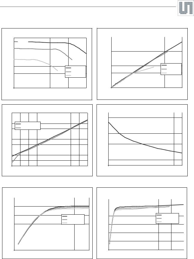
Figure 6. LIN to HPH: THD+N vs. Output Power
THD+N vs POUT - 16Ω - single ended stereo
|
1 |
|
|
|
|
|
|
|
|
|
|
|
|
VBAT=1.8V |
|
|
|
|
|
|
|
VBAT=1.5V |
|
|
|
|
|
|
|
VBAT=1.0V |
|
[%] |
|
|
|
|
|
|
|
THD+N |
0,1 |
|
|
|
|
|
|
|
|
|
|
|
|
|
|
|
0,01 |
|
|
|
|
|
|
|
0 |
10 |
20 |
30 |
40 |
50 |
60 |
Pout [mW]
|
|
THD+N vs POUT - 32Ω - bridged-tied load |
|
|
||||||||||
|
1 |
|
|
|
|
|
|
|
|
|
|
|
|
|
|
|
|
|
|
|
|
VBAT=1.8V |
|
|
|
|
|
|
|
|
|
|
|
|
|
|
VBAT=1.5V |
|
|
|
|
|
|
|
|
|
|
|
|
|
|
VBAT=1.0V |
|
|
|
|
|
|
|
[%] |
|
|
|
|
|
|
|
|
|
|
|
|
|
|
THD+N |
0,1 |
|
|
|
|
|
|
|
|
|
|
|
|
|
|
|
|
|
|
|
|
|
|
|
|
|
|
|
|
|
0,01 |
|
|
|
|
|
|
|
|
|
|
|
|
|
|
0 |
10 |
20 |
30 |
40 |
50 |
60 |
70 |
80 |
90 |
100 |
110 |
120 |
130 |
|
|
|
|
|
|
|
Pout [mW] |
|
|
|
|
|
|
|
THD+N vs POUT - 32Ω - stereo single ended
|
1 |
|
|
|
|
|
|
|
|
|
|
|
|
|
|
|
|
VBAT=1.8V |
|
|
|
|
|
|
|
|
|
VBAT=1.5V |
|
|
|
|
|
|
|
|
|
VBAT=1.0V |
|
[%] |
|
|
|
|
|
|
|
|
|
THD+N |
0,1 |
|
|
|
|
|
|
|
|
|
|
|
|
|
|
|
|
|
|
|
0,01 |
|
|
|
|
|
|
|
|
|
0 |
5 |
10 |
15 |
20 |
25 |
30 |
35 |
40 |
Pout [mW]
|
|
THD+N vs POUT - 64Ω - bridged-tied load |
|
|
||||||
|
1 |
|
|
|
|
|
|
|
|
|
|
|
|
|
|
VBAT=1.8V |
|
|
|
|
|
|
|
|
|
|
VBAT=1.5V |
|
|
|
|
|
|
|
|
|
|
VABT=1.0V |
|
|
|
|
|
[%] |
|
|
|
|
|
|
|
|
|
|
THD+N |
0,1 |
|
|
|
|
|
|
|
|
|
|
|
|
|
|
|
|
|
|
|
|
|
0,01 |
|
|
|
|
|
|
|
|
|
|
0 |
10 |
20 |
30 |
40 |
50 |
60 |
70 |
80 |
90 |
|
|
|
|
|
Pout [mW] |
|
|
|
|
|
Figure 7. VNEG Charge Pump |
|
|
|
|
|
|
|
|
|
|
|
|
|
|
||
|
|
VNEG CP Voltage vs Load Current |
|
|
|
|
VNEG CP Efficiency |
|
|
|
|
|||||
|
0,0 |
|
|
|
|
100 |
|
|
|
|
|
|
|
|
|
|
|
-0,2 |
|
|
VBAT=1.0V |
|
95 |
|
|
|
|
|
|
|
|
|
|
|
|
|
|
|
|
|
|
|
|
|
|
|
|
|
|
|
|
-0,4 |
|
|
VBAT=1.5V |
|
90 |
|
|
|
|
|
|
|
|
|
|
|
|
|
|
VBAT=1.8V |
|
85 |
|
|
|
|
|
|
|
|
|
|
|
-0,6 |
|
|
|
|
|
|
|
|
|
|
|
|
|
|
|
[V] |
|
|
|
|
|
|
|
|
|
|
|
|
|
|
|
|
-0,8 |
|
|
|
|
80 |
|
|
|
|
|
|
|
|
|
|
|
VNEGV |
|
|
|
[%]Eff |
|
|
|
|
|
|
|
|
|
|
||
|
|
|
70 |
|
|
|
|
|
|
|
|
|
|
|||
|
|
|
|
|
|
|
|
|
|
|
|
|
|
|||
|
-1,0 |
|
|
|
|
75 |
|
|
|
|
|
|
|
|
|
|
|
|
|
|
|
|
|
|
|
|
|
|
|
|
|
|
|
|
-1,2 |
|
|
|
|
65 |
|
|
|
|
|
|
|
|
|
|
|
|
|
|
|
|
|
|
|
|
|
|
|
VBAT=1.0V |
|
||
|
-1,4 |
|
|
|
|
|
|
|
|
|
|
|
|
|
||
|
|
|
|
|
60 |
|
|
|
|
|
|
|
VBAT=1.5V |
|
||
|
|
|
|
|
|
|
|
|
|
|
|
|
|
|||
|
|
|
|
|
|
|
|
|
|
|
|
|
VBAT=1.8V |
|
||
|
-1,6 |
|
|
|
|
|
|
|
|
|
|
|
|
|
||
|
|
|
|
|
55 |
|
|
|
|
|
|
|
|
|
|
|
|
|
|
|
|
|
|
|
|
|
|
|
|
|
|
|
|
|
-1,8 |
|
|
|
|
50 |
|
|
|
|
|
|
|
|
|
|
|
0 |
50 |
100 |
150 |
200 |
|
|
|
|
|
|
|
|
|
|
|
|
0 |
20 |
40 |
60 |
80 |
100 |
120 |
140 |
160 |
180 |
200 |
|||||
|
|
|
|
|
|
|||||||||||
|
|
|
I_VNEG [mA] |
|
|
|
|
|
|
I_VNEG [mA] |
|
|
|
|
||
www.ams.com/ANC |
|
|
Revision 1.10 |
|
|
|
|
|
|
|
|
11 - 53 |
||||
AS3400/10/30
Data Sheet - Ty p i c a l O p e r a t i n g C h a r a c t e r i s t i c s
Figure 8. Microphone Supply Generation
MICS Charge Pump
|
3,5 |
|
|
|
|
|
3 |
|
|
|
|
|
2,5 |
|
|
|
|
[V] |
2 |
|
|
|
|
MICS |
|
|
|
|
|
1,5 |
|
|
|
VBAT=1.8V |
|
V |
|
|
|
|
|
|
1 |
|
|
|
VBAT=1.5V |
|
|
|
|
VABT=1.0V |
|
|
|
|
|
|
|
|
0,5 |
|
|
|
|
|
0 |
|
|
|
|
|
0 |
500 |
1000 |
1500 |
2000 |
|
|
|
I_MICS [uA] |
|
|
|
|
|
|
V_MICS vs V_VBAT |
|
|
|
|||
|
3,5 |
|
|
|
|
|
|
|
|
|
|
3,3 |
|
|
|
|
|
|
|
|
|
|
3,1 |
I_MCS = 0.0uA |
|
|
|
|
|
|
||
|
2,9 |
I_MICS = 600uA |
|
|
|
|
|
|
||
|
|
|
|
|
|
|
|
|
|
|
[V] |
2,7 |
|
|
|
|
|
|
|
|
|
|
|
|
|
|
|
|
|
|
|
|
MICS |
2,5 |
|
|
|
|
|
|
|
|
|
2,3 |
|
|
|
|
|
|
|
|
|
|
V |
|
|
|
|
|
|
|
|
|
|
|
2,1 |
|
|
|
|
|
|
|
|
|
|
1,9 |
|
|
|
|
|
|
|
|
|
|
1,7 |
|
|
|
|
|
|
|
|
|
|
1,5 |
|
|
|
|
|
|
|
|
|
|
0,9 |
1,0 |
1,1 |
1,2 |
1,3 |
1,4 |
1,5 |
1,6 |
1,7 |
1,8 |
VBAT [V]
I_MICS vs dI_VBAT
|
7000 |
|
|
|
|
|
6000 |
|
|
|
|
|
5000 |
|
|
|
|
[uA] |
4000 |
|
|
|
|
VBAT |
|
|
|
|
|
3000 |
|
|
VBAT=1.8V |
||
dI_ |
|
|
|
VBAT=1.5V |
|
|
2000 |
|
|
VBAT=1.0V |
|
|
1000 |
|
|
|
|
|
0 |
|
|
|
|
|
0 |
500 |
1000 |
1500 |
2000 |
|
|
|
I_MICS [uA] |
|
|
|
|
|
R_MICS_Switch vs V_VBAT |
|
|
|
||||
|
140 |
|
|
|
|
|
|
|
|
|
|
130 |
|
|
|
|
|
|
|
|
|
|
120 |
|
|
|
|
|
|
|
|
|
] |
110 |
|
|
|
|
|
|
|
|
|
[Ω |
|
|
|
|
|
|
|
|
|
|
|
|
|
|
|
|
|
|
|
|
|
Switch |
100 |
|
|
|
|
|
|
|
|
|
90 |
|
|
|
|
|
|
|
|
|
|
_ |
|
|
|
|
|
|
|
|
|
|
R MICS |
80 |
|
|
|
|
|
|
|
|
|
70 |
|
|
|
|
|
|
|
|
|
|
|
60 |
|
|
|
|
|
|
|
|
|
|
50 |
|
|
|
|
|
|
|
|
|
|
40 |
|
|
|
|
|
|
|
|
|
|
0,9 |
1,0 |
1,1 |
1,2 |
1,3 |
1,4 |
1,5 |
1,6 |
1,7 |
1,8 |
VBAT [V]
Figure 9. ILED Current Sink (100% PWM setting)
ILED Current
|
120,0 |
|
|
|
|
|
|
100,0 |
|
|
|
|
|
|
80,0 |
|
|
|
ILED (Vbat=1.8V) |
|
|
|
|
|
|
|
|
[%] |
|
|
|
|
ILED (Vbat=1.5V) |
|
|
|
|
|
ILED (Vbat=1.0V) |
|
|
I (ILED) |
60,0 |
|
|
|
|
|
|
|
|
|
|
||
|
|
|
|
|
|
|
|
40,0 |
|
|
|
|
|
|
20,0 |
|
|
|
|
|
|
0,0 |
|
|
|
|
|
|
0,0 |
0,1 |
0,2 |
0,3 |
0,4 |
0,5 |
|
|
|
V (ILED-VNEG) [V] |
|
|
|
ILED Current
|
120,0 |
|
|
|
|
|
|
|
100,0 |
|
|
|
|
|
|
|
80,0 |
|
|
|
|
ILED (Vbat=1.8V) |
|
|
|
|
|
|
|
|
|
[%] |
|
|
|
|
|
ILED (Vbat=1.5V) |
|
|
|
|
|
|
ILED (Vbat=1.0V) |
|
|
I (ILED) |
|
|
|
|
|
|
|
60,0 |
|
|
|
|
|
|
|
|
|
|
|
|
|
|
|
|
40,0 |
|
|
|
|
|
|
|
20,0 |
|
|
|
|
|
|
|
0,0 |
|
|
|
|
|
|
|
0,0 |
0,5 |
1,0 |
1,5 |
2,0 |
2,5 |
3,0 |
|
|
|
|
V (ILED-VNEG) [V] |
|
|
|
www.ams.com/ANC |
Revision 1.10 |
12 - 53 |
AS3400/10/30
Data Sheet - Ty p i c a l O p e r a t i n g C h a r a c t e r i s t i c s
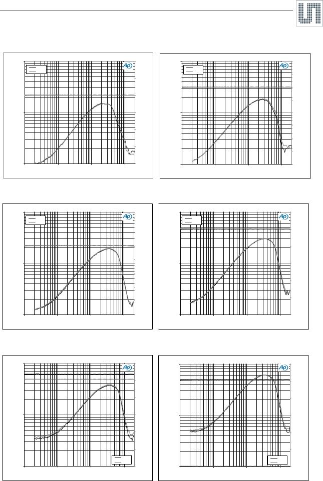
Figure 10. THD+N and Output Power(20mW) versus Frequency with 32Ω load
0,1 |
|
|
30 |
|
|
Left |
|
|
|
|
Right |
|
|
|
|
|
|
25 |
|
THD+N[%] |
|
|
20 |
PowerOutput[mW] |
|
|
|
||
0,01 |
|
|
15 |
|
|
|
|
10 |
|
|
|
|
5 |
|
0,001 |
|
|
0 |
|
10 |
100 |
1000 |
10000 |
|
f [Hz]
Figure 11. THD+N and Output Power(30mW) versus Frequency with 16Ω load
0,1 |
|
|
40 |
|
|
Left |
|
|
|
|
Right |
|
35 |
|
|
|
|
|
|
|
|
|
30 |
|
THD+N[%] |
|
|
25 |
PowerOutput[mW] |
|
|
|
||
0,01 |
|
|
20 |
|
|
|
|
15 |
|
|
|
|
10 |
|
|
|
|
5 |
|
0,001 |
|
|
0 |
|
10 |
100 |
1000 |
10000 |
|
f [Hz]
Figure 12. THD+N and Output Power(10mW) versus Frequency with 32Ω load
0,1 |
|
|
|
|
|
Left |
|
14 |
|
|
|
|
|
|
|
Right |
|
|
|
|
|
|
12 |
|
THD+N[%] |
|
|
10 |
PowerOutput[mW] |
|
|
8 |
||
0,01 |
|
|
|
|
|
|
|
6 |
|
|
|
|
4 |
|
|
|
|
2 |
|
0,001 |
|
|
0 |
|
10 |
100 |
1000 |
10000 |
|
f [Hz]
Figure 13. THD+N and Output Power(10mW) versus Frequency with 16Ω load
0,1 |
|
|
12 |
|
|
Left |
|
|
|
|
Right |
|
|
|
|
|
|
10 |
|
THD+N[%] |
|
|
8 |
PowerOutput[mW] |
|
|
|
||
0,01 |
|
|
6 |
|
|
|
|
4 |
|
|
|
|
2 |
|
0,001 |
|
|
0 |
|
10 |
100 |
1000 |
10000 |
|
f [Hz]
Figure 14. THD+N and Output Power(1mW) versus |
Figure 15. THD+N and Output Power(1mW) versus |
Frequency with 32Ω load |
Frequency with 16Ω load |
THD+N [%]
0,1 |
|
|
1,2 |
|
|
|
1 |
|
|
|
0,8 |
0,01 |
|
|
0,6 |
|
|
|
0,4 |
|
|
|
0,2 |
|
|
|
Left |
|
|
|
Right |
0,001 |
|
|
0 |
10 |
100 |
1000 |
10000 |
f [Hz]
Output Power [mW]
THD+N [%]
0,1 |
|
|
1,2 |
|
|
|
1 |
|
|
|
0,8 |
0,01 |
|
|
0,6 |
|
|
|
0,4 |
|
|
|
0,2 |
|
|
|
Left |
|
|
|
Right |
0,001 |
|
|
0 |
10 |
100 |
1000 |
10000 |
f [Hz]
Output Power [mW]
www.ams.com/ANC |
Revision 1.10 |
13 - 53 |
AS3400/10/30
Data Sheet - Ty p i c a l O p e r a t i n g C h a r a c t e r i s t i c s
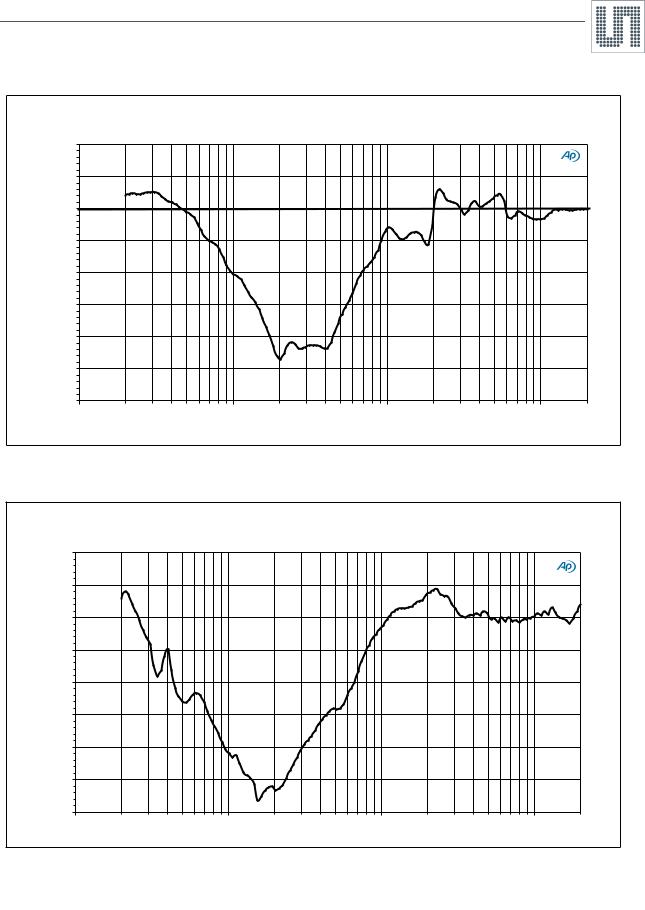
Figure 16. Typical Performance Data, Feed Forward configuration with an over the ear headset
ANC Performance [dB]
Feed Forward Topology - Over the Ear Headset
10
5
0
-5
-10
-15
-20
-25
-30
10 |
100 |
1000 |
10000 |
f [Hz]
Figure 17. Typical Performance Data, Feedback configuration with an on ear headset
Feedback Topology - On Ear Headset
ANC Performance [dB]
10
5
0 
-5
-10
-15
-20
-25
-30
10 |
100 |
1000 |
10000 |
f [Hz]
www.ams.com/ANC |
Revision 1.10 |
14 - 53 |
AS3400/10/30
Data Sheet - D e t a i l e d D e s c r i p t i o n
8 Detailed Description
This section provides a detailed description of the device related components.
8.1 Audio Line Input
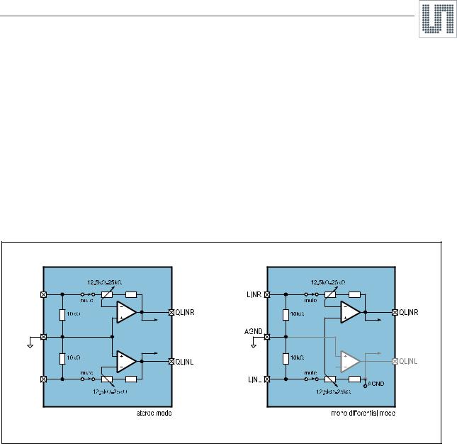
The chip features one line input. The blocks can work in mono differential or in stereo single ended mode.
In addition to the 12.5-25kΩ input impedance, LineIn has a termination resistor of 10kΩ which is also effective during MUTE to charge eventually given input capacitors.
8.1.1Gain Stage
The Line In gain stage is designed to have 63 gain steps of 0.75dB with a max gain of 0dB plus MUTE.
In default, the gain will be ramped up from MUTE to 0dB during startup. There is a possibility to make the playback volume user controlled by the VOL pin with an ADC converted VOL voltage or UP/DN buttons.
In monitor mode, the gain stage can be set to an fixed default attenuation level for reducing the loudness of the music.
Figure 18. Line Inputs
8.1.2Parameter
VBAT=1.5V, TA= 25ºC, unless otherwise specified.
Table 4. Line Input Parameter
Symbol |
Parameter |
Condition |
Min |
Typ |
Max |
Unit |
VLIN |
Input Signal Level |
|
|
0.6* |
VBAT |
VPEAK |
|
|
VBAT |
||||
|
|
|
|
|
|
|
|
|
|
|
|
|
|
|
|
0dB gain (12.5k // 10k) |
|
5.6 |
|
kΩ |
RLIN |
Input Impedance |
|
|
|
|
|
-46.5dB gain (25k // 10k) |
|
7.2 |
|
kΩ |
||
|
|
MUTE |
|
10 |
|
kΩ |
|
|
|
|
|
|
|
∆RLIN |
Input Impedance Tolerance |
|
|
±30 |
|
% |
CLIN |
Input Capacitance |
|
|
5 |
|
pF |
ALIN |
Programmable Gain |
|
-46.5 |
|
+0 |
dB |
|
Gain Steps |
Discrete logarithmic gain steps |
|
0.75 |
|
dB |
|
|
|
|
|
|
|
|
Gain Step Accuracy |
|
|
0.5 |
|
dB |
|
|
|
|
|
|
|
ALINMUTE |
Mute Attenuation |
|
|
100 |
|
dB |
www.ams.com/ANC |
Revision 1.10 |
15 - 53 |

AS3400/10/30
Data Sheet - D e t a i l e d D e s c r i p t i o n
Table 4. Line Input Parameter (Continued)
Symbol |
Parameter |
Condition |
Min |
Typ |
Max |
Unit |
|
|
PotiMode, Tinit=100ms |
|
20 |
|
|
∆ALIN |
Gain Ramp Rate |
|
|
|
|
|
ButtonMode, Tinit=400ms |
|
80 |
|
ms/step |
||
|
|
MonitorMode |
|
8 |
|
|
|
|
|
|
|
|
|
VATTACK |
Limiter Activation Level |
HPL/R start of neg. clipping |
|
|
|
VPEAK |
VDECAY |
Limiter Release Level |
HPL/R |
|
VNEG |
|
VPEAK |
|
+0.3 |
|
||||
|
|
|
|
|
|
|
|
|
|
|
|
|
|
tATTACK |
Limiter Attack Time |
|
|
4 |
|
µs |
tDECAY |
Limiter Decay Time |
|
|
8 |
|
ms |
8.2 Microphone Input
The AFE offers two microphone inputs and one low noise microphone voltage supply (microphone bias). The inputs can be switched to single ended or differential mode.
Figure 19. Microphone Input
8.2.1Gain Stage & Limiter
The Mic GainStage has programmable Gain within -6dB…+41.625dB in 128 steps of 0.375dB.
As soft-start function is implemented for an automatic gain ramping implemented with steps of 4ms to fade in the audio at the end of the start-up sequence.
A limiter automatically attenuates high input signals. The AGC has 127 steps with 0.375dB with a dynamic range of the full gain stage. In monitor mode, the gain stage can be set to an fixed (normally higher) gain level or be controlled by the VOL pin.
8.2.2Supply
The MICS charge pump is providing a proper microphone supply voltage for the AAA supply. Since AAA batteries are operating down to 1.0V, the direct battery voltage cannot be used for mic-supply. There are 2 modes.
The first mode SWITCH-MODE for 1.8V supply is to have just a switch from VBAT to MICS. With this switch, the microphone current is switched off in idle mode.
The second mode CHAREGPUMP_MODE for AAA batteries is the real charge pump mode, in this mode a positive voltage is generated of about 2* VBAT.
It is also possible to switch off the microphone supply if not needed (e.g. playback without ANC)
www.ams.com/ANC |
Revision 1.10 |
16 - 53 |

AS3400/10/30
Data Sheet - D e t a i l e d D e s c r i p t i o n
8.2.3Parameter
VBAT=1.5V, TA= 25ºC unless otherwise specified.
Table 5. Microphone Input Parameter
Symbol |
Parameter |
Condition |
Min |
Typ |
Max |
Unit |
VMICIN0 |
Input Signal Level |
AMIC = 30dB |
|
20 |
|
mVP |
VMICIN1 |
|
AMIC = 36dB |
|
10 |
|
mVP |
VMICIN2 |
|
AMIC = 42dB |
|
5 |
|
mVP |
RMICIN |
Input Impedance |
MICP to AGND |
|
7.5 |
|
kΩ |
∆MICIN |
Input Impedance Tolerance |
|
|
-7 |
|
% |
|
|
+33 |
|
|||
|
|
|
|
|
|
|
|
|
|
|
|
|
|
CMICIN |
Input Capacitance |
|
|
5 |
|
pF |
AMIC |
Programmable Gain |
|
-6 |
|
+41.6 |
dB |
|
Gain Steps |
Discrete logarithmic gain steps |
|
0.375 |
|
dB |
|
|
|
|
|
|
|
|
Gain Step Precision |
|
|
0.15 |
|
dB |
|
|
|
|
|
|
|
∆AMIC |
Gain Ramp Rate |
Tinit=64ms |
|
4 |
|
ms/step |
VATTACK |
Limiter Activation Level |
VPEAK related to VBAT or VNEG |
|
0.67 |
|
1 |
VDECAY |
Limiter Release Level |
|
0.4 |
|
1 |
|
|
|
|
||||
AMICLIMIT |
Limiter Gain Overdrive |
127 @ 0.375dB |
|
41.625 |
|
dB |
tATTACK |
Limiter Attack Time |
|
|
5 |
|
µs/step |
tDECAY-DEB |
Limiter Decay Debouncing Time |
|
|
64 |
|
ms |
tDECAY |
Limiter Decay Time |
|
|
4 |
|
ms/step |
|
|
|
|
|
|
|
VMICS |
Microphone Supply Voltage |
|
|
VBAT*2- |
|
V |
|
|
240mV |
|
|||
|
|
|
|
|
|
|
|
|
|
|
|
|
|
|
|
VBAT=+1.0V |
|
|
|
|
IMICSMIN |
Min. Microphone Supply Current |
VNEG=-0.7V |
|
650 |
|
µA |
|
|
MICS=+1.75V |
|
|
|
|
|
|
|
|
|
|
|
ROUT_CP |
CP Output Resistance |
|
|
1300 |
|
Ω |
www.ams.com/ANC |
Revision 1.10 |
17 - 53 |
AS3400/10/30
Data Sheet - D e t a i l e d D e s c r i p t i o n
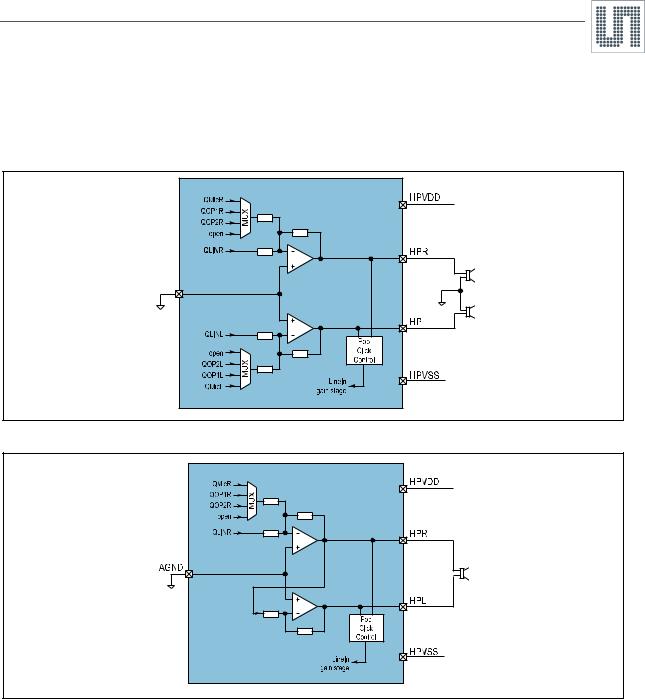
8.3 Headphone Output
The headphone output is a true ground output using VNEG as negative supply, designed to provide the audio signal with 2x12mW @ 16Ω-64Ω, which are typical values for headphones. It is also capable to operate in bridged mode for higher impedance (e.g. 300Ω) headphone. In this mode the left output is carrying the inverted signal of the right output shown in Figure 21.
Figure 20. Headphone Output Single Ended Mode
Figure 21. Headphone Output Differential Mode
8.3.1Input Multiplexer
The signal from the line-input gain stage gets summed at the input of the headphone stage with the microphone gain stage output, the first filter opamp output or the second filter opamp output. The microphone gain stage output is used per default. It is also possible to playback without ANC by only using the line-input gain stage with no other signal on the multiplexer.
For the monitor mode, the setting of this input multiplexer can be changed to another source, normally to the microphone.
8.3.2No-Pop Function
The No-Pop startup of the headphone stage takes 60ms to 120ms dependent on the supply voltage.
8.3.3No-Clip Function
The headphone output stage gets monitored by comparator stages which detect if the output signal starts to clip.
This signal is used to reduce the LineIn gain to avoid distortion of the output signal. A hystereses avoids jumping between 2 gain steps for a signal with constant amplitude.
www.ams.com/ANC |
Revision 1.10 |
18 - 53 |
AS3400/10/30
Data Sheet - D e t a i l e d D e s c r i p t i o n
8.3.4Over-Current Protection
The over-current protection has a threshold of 150-200mA and a debouncing time of 8µs. The stage is forced to OFF mode in an over-current situation. After this, the headphone stage tries to power up again every 8ms as long as the over-current situation still exists or the stage is turned off manually.
8.3.5Parameter
VBAT=1.5V, TA= 25ºC, unless otherwise specified.
Table 6. Headphone Output Parameter
Symbol |
Parameter |
Condition |
Min |
Typ |
Max |
Unit |
RL_HP |
Load Impedance |
Stereo mode |
16 |
|
|
Ω |
CL_HP |
Load Capacitance |
Stereo mode |
|
|
100 |
pF |
|
|
RL=64Ω |
12 |
|
|
mW |
|
|
|
|
|
|
|
PHP |
Nominal Output Power |
RL=32Ω |
24 |
|
|
mW |
|
|
RL=16Ω |
34 |
|
|
mW |
|
|
|
|
|
|
|
PSRRHP |
Power Supply Rejection Ratio |
200Hz-20kHz, 720mVpp, RL=16Ω |
|
90 |
|
dB |
8.4 Operational Amplifier
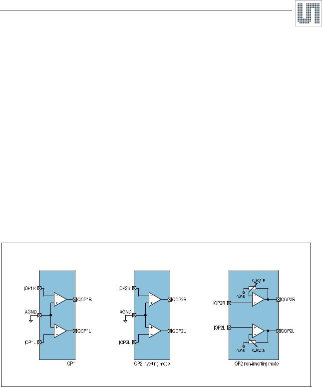
While AS3410 offers only one operational amplifier for feed-forward ANC, AS3400 and AS3430 feature an additional second operational amplifier stage to perform feed-back ANC or any other additional needed filtering.
Both operational amplifiers stages can be activated and used individually. While OP1 stage is always configured as inverting amplifier, OP2 stage can be also switched to a non-inverting mode with an adjustable gain of 0...+10.5dB.
Figure 22. Operational Amplifiers
www.ams.com/ANC |
Revision 1.10 |
19 - 53 |

AS3400/10/30
Data Sheet - D e t a i l e d D e s c r i p t i o n
8.4.1Parameter
VBAT=1.5V, TA= 25ºC, unless otherwise specified.
Table 7. Headphone Output Parameter
Symbol |
Parameter |
Condition |
Min |
Typ |
Max |
Unit |
RL_OP |
Load Impedance |
Single ended |
1 |
|
|
kΩ |
CL_OP |
Load Capacitance |
Single ended |
|
|
100 |
pF |
GBWOP |
Gain Band Width |
|
|
4.3 |
|
MHz |
|
|
|
|
|
|
|
VOS_OP |
Offset Voltage |
|
|
|
6 |
mV |
VEIN_HP |
Equivalent Input Noise |
200Hz-20kHz |
|
2.6 |
|
µV |
www.ams.com/ANC |
Revision 1.10 |
20 - 53 |