

Fundamentals of Microelectronics
.pdfBR |
Wiley/Razavi/Fundamentals of Microelectronics [Razavi.cls v. 2006] |
June 30, 2007 at 13:42 |
51 (1) |
|
|
|
|
Sec. 2.2 |
P N Junction |
51 |
Thus, a tenfold increase in the device area lowers the voltage by 60 mV if ID remains constant.
Exercise
A diode in forward bias with ID IS exp(VD =VT ) undergoes two simultaneous changes: the current is raised by a factor of m and the area is increased by a factor of n. Determine the change in the device voltage.
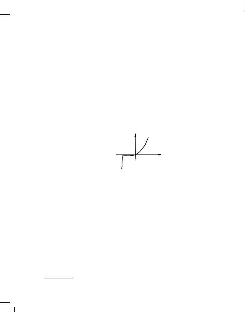
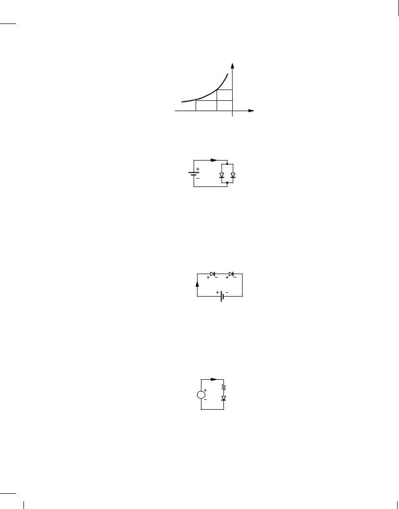
Constant-Voltage Model The exponential I/V characteristic of the diode results in nonlinear equations, making the analysis of circuits quite difficult. Fortunately, the above examples imply that the diode voltage is a relatively weak function of the device current and cross section area. With typical current levels and areas, VD falls in the range of 700 - 800 mV. For this reason, we often approximate the forward bias voltage by a constant value of 800 mV (like an ideal battery), considering the device fully off if VD < 800 mV. The resulting characteristic is illustrated in Fig. 2.33(a) with the turn-on voltage denoted by VD;on. Note that the current goes to infinity as VD tends to exceed VD;on because we assume the forward-biased diode operates as an ideal voltage source. Neglecting the leakage current in reverse bias, we derive the circuit model shown in Fig. 2.33(b). We say the junction operates as an open circuit if VD < VD;on and as a constant voltage source if we attempt to increase VD beyond VD;on. While not essential, the voltage source placed in series with the switch in the off condition helps simplify the analysis of circuits: we can say that in the transition from off to on, only the switch turns on and the battery always resides in series with the switch.
Reverse Bias
I D
|
|
VD,on |
|
|
Forward Bias |
VD,on |
VD |
VD,on |
|
|
|
(a) |
|
(b) |
Figure 2.33 Constant-voltage diode model.
A number of questions may cross the reader's mind at this point. First, why do we subject the diode to such a seemingly inaccurate approximation? Second, if we indeed intend to use this simple approximation, why did we study the physics of semiconductors and pn junctions in such detail?
The developments in this chapter are representative of our treatment of all semiconductor devices: we carefully analyze the structure and physics of the device to understand its operation; we construct a “physics-based” circuit model; and we seek to approximate the resulting model, thus arriving at progressively simpler representations. Device models having different levels of complexity (and, inevitably, different levels of accuracy) prove essential to the analysis and design of circuits. Simple models allow a quick, intuitive understanding of the operation of a complex circuit, while more accurate models reveal the true performance.
Example 2.21
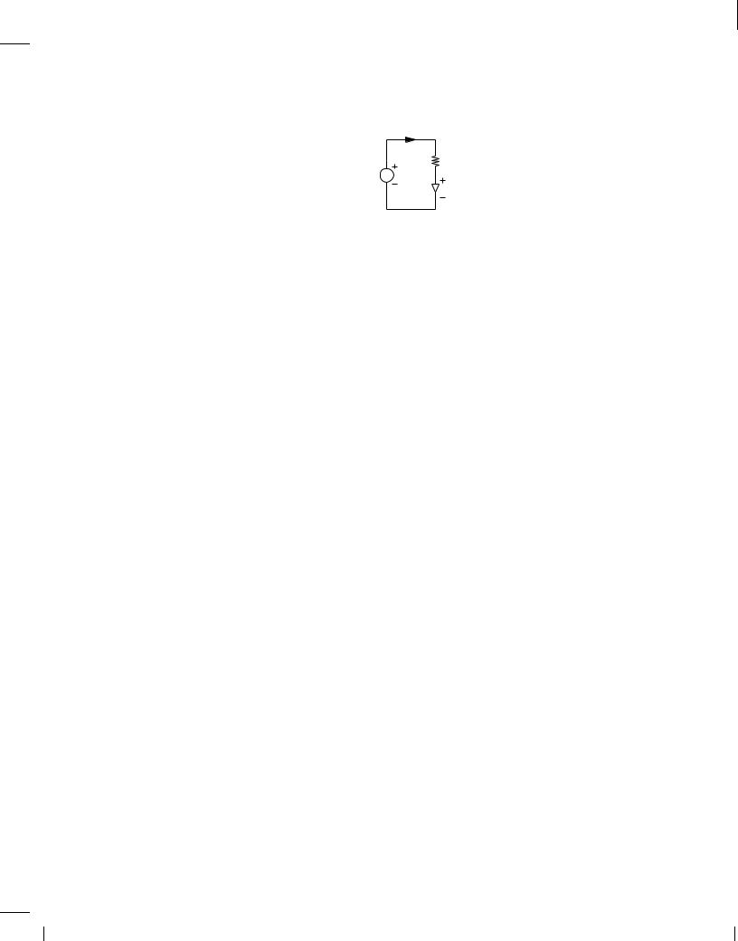
Consider the circuit of Fig. 2.34. Calculate IX for VX = 3 V and VX = 1 V using (a) an exponential model with IS = 10,16 A and (b) a constant-voltage model with VD;on = 800 mV.
BR |
Wiley/Razavi/Fundamentals of Microelectronics [Razavi.cls v. 2006] |
June 30, 2007 at 13:42 |
52 (1) |
|
|
|
|
52 |
Chap. 2 |
Basic Physics of Semiconductors |
I X
R1 = 1 kΩ
VX
D1  VD
VD
Figure 2.34 Simple circuit using a diode.
Solution
(a) Noting that ID = IX , we have
VX |
= |
IX R1 + VD |
VD = VT ln IX :
IS
(2.114)
(2.115)
This equation must be solved by iteration: we guess a value for VD, compute the corresponding IX from IX R1 = VX , VD, determine the new value of VD from VD = VT ln(IX =IS) and iterate. Let us guess VD = 750 mV and hence
IX = |
VX , VD |
(2.116) |
|
R1 |
|
= |
3 V , 0:75 V |
(2.117) |
|
1 k |
|
= 2:25 mA: |
(2.118) |
|
Thus, |
|
|
VD |
= VT ln IX |
(2.119) |
|
IS |
|
|
= 799 mV: |
(2.120) |
With this new value of VD, we can obtain a more accurate value for IX : |
|
|
I = 3 V , 0:799 V |
(2.121) |
|
X |
1 k |
|
|
|
|
= 2:201 mA: |
(2.122) |
|
We note that the value of IX rapidly converges. Following the same procedure for VX = 1 V, we have
IX = |
1 V , 0:75 V |
(2.123) |
|
1 k |
|
= |
0:25 mA; |
(2.124) |
which yields VD = 0:742 V and hence IX = 0:258 mA. (b) A constant-voltage model readily gives
IX = 2:2 mA for VX = 3 V |
(2.125) |
IX = 0:2 mA for VX = 1 V: |
(2.126) |
BR |
Wiley/Razavi/Fundamentals of Microelectronics [Razavi.cls v. 2006] |
June 30, 2007 at 13:42 |
53 (1) |
|
|
|
|
Sec. 2.3 |
Reverse Breakdown |
53 |
The value of IX incurs some error, but it is obtained with much less computational effort than that in part (a).
Exercise
Repeat the above example if the cross section area of the diode is increased by a factor of 10.
2.3 Reverse Breakdown
Recall from Fig. 2.31 that the pn junction carries only a small, relatively constant current in reverse bias. However, as the reverse voltage across the device increases, eventually “breakdown” occurs and a sudden, enormous current is observed. Figure 2.35 plots the device I/V characteristic, displaying this effect.
I D
VBD
VD
Breakdown
Figure 2.35 Reverse breakdown characteristic.
The breakdown resulting from a high voltage (and hence a high electric field) can occur in any material. A common example is lightning, in which case the electric field in the air reaches such a high level as to ionize the oxygen molecules, thus lowering the resistance of the air and creating a tremendous current.
The breakdown phenomenon in pn junctions occurs by one of two possible mechanisms: “Zener effect” and “avalanche effect.”
2.3.1 Zener Breakdown
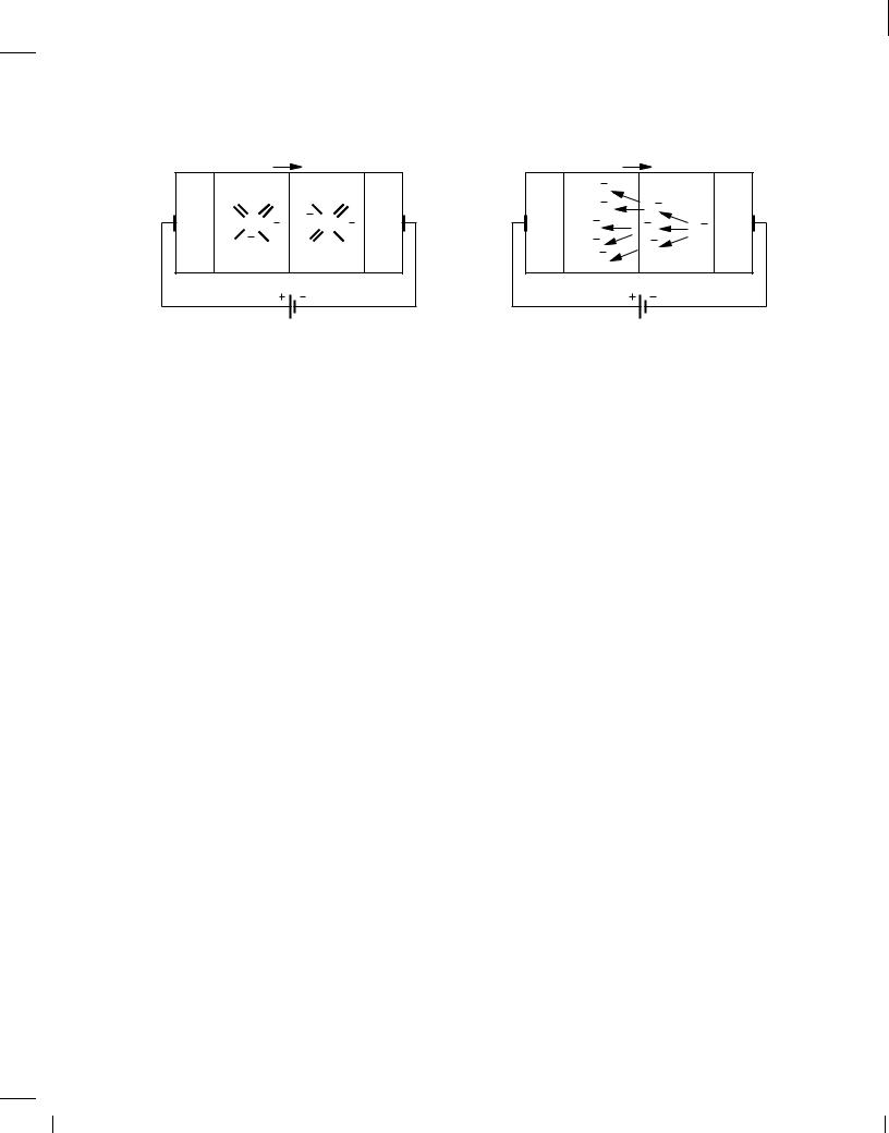
The depletion region in a pn junction contains atoms that have lost an electron or a hole and, therefore, provide no loosely-connected carriers. However, a high electric field in this region may impart enough energy to the remaining covalent electrons to tear them from their bonds [Fig. 2.36(a)]. Once freed, the electrons are accelerated by the field and swept to the n side of the junction. This effect occurs at a field strength of about 106 V/cm (1 V/ m).
In order to create such high fields with reasonable voltages, a narrow depletion region is required, which from Eq. (2.76) translates to high doping levels on both sides of the junction (why?). Called the “Zener effect,” this type of breakdown appears for reverse bias voltages on the order of 3-8 V.
This section can be skipped in a first reading.
BR |
Wiley/Razavi/Fundamentals of Microelectronics [Razavi.cls v. 2006] |
June 30, 2007 at 13:42 |
54 (1) |
|
|
|
|
54 |
|
|
|
Chap. 2 |
Basic Physics of Semiconductors |
||
n |
E |
|
p |
n |
|
E |
p |
|
|
|
|
||||
Si |
Si |
Si |
Si |
|
e |
|
|
|
e |
e |
|
||||
|
|
e |
|
|
|
||
Si |
e |
Si e |
|
e |
e |
e |
|
|
|
||||||
Si e |
Si |
Si |
Si |
|
e |
e |
|
|
|
|
|
|
e |
|
|
|
VR |
|
|
|
VR |
|
|
|
(a) |
|
|
|
|
(b) |
|
|
|
|
|
|
|
|
|
Figure 2.36 (a) Release of electrons due to high electric field, (b) avalanche effect.
2.3.2 Avalanche Breakdown
Junctions with moderate or low doping levels (< 1015 cm3) generally exhibit no Zener breakdown. But, as the reverse bias voltage across such devices increases, an avalanche effect takes place. Even though the leakage current is very small, each carrier entering the depletion region experiences a very high electric field and hence a large acceleration, thus gaining enough energy to break the electrons from their covalent bonds. Called “impact ionization,” this phenomenon can lead to avalanche: each electron freed by the impact may itself speed up so much in the field as to collide with another atom with sufficient energy, thereby freeing one more covalent-bond electron. Now, these two electrons may again acquire energy and cause more ionizing collisions, rapidly raising the number of free carriers.
An interesting contrast between Zener and avalanche phenomena is that they display opposite temperature coefficients (TCs): VBD has a negative TC for Zener effect and positive TC for avalanche effect. The two TCs cancel each other for VBD 3:5 V. For this reason, Zener diodes with 3.5-V rating find application in some voltage regulators.
The Zener and avalanche breakdown effects do not damage the diodes if the resulting current remains below a certain limit given by the doping levels and the geometry of the junction. Both the breakdown voltage and the maximum allowable reverse current are specified by diode manufacturers.
2.4Chapter Summary
Silicon contains four atoms in its last orbital. It also contains a small number of free electrons at room temperature.
When an electron is freed from a covalent bond, a “hole” is left behind.
The bandgap energy is the minimum energy required to dislodge an electron from its covalent bond.
To increase the number of free carriers, semiconductors are “doped” with certain impurities. For example, addition of phosphorous to silicon increases the number of free electrons because phosphorous contains five electrons in its last orbital.
For doped or undoped semiconductors, np = n2. For example, in an n-type material, |
|
|
i |
n N and hence p n2=ND. |
|
D |
i |
Charge carriers move in semiconductors via two mechanisms: drift and diffusion.
BR |
Wiley/Razavi/Fundamentals of Microelectronics [Razavi.cls v. 2006] |
June 30, 2007 at 13:42 |
55 (1) |
|
|
|
|
Sec. 2.4 |
Chapter Summary |
55 |
The drift current density is proportional to the electric field and the mobility of the carriers and is given by Jtot = q( nn + pp)E.
The diffusion current density is proportional to the gradient of the carrier concentration and given by Jtot = q(Dndn=dx , Dpdp=dx).
A pn junction is a piece of semiconductor that receives n-type doping in one section and p-type doping in an adjacent section.
The pn junction can be considered in three modes: equilibrium, reverse bias, and forward bias.
Upon formation of the pn junction, sharp gradients of carrier densities across the junction result in a high current of electrons and holes. As the carriers cross, they leave ionized atoms behind, and a “depletion resgion” is formed. The electric field created in the depletion region eventually stops the current flow. This condition is called equilibrium.
The electric field in the depletion results in a built-in potential across the region equal to
(kT=q) ln(NAND)=n2, typically in the range of 700 to 800 mV.
i
Under reverse bias, the junction carries negligible current and operates as a capacitor. The capacitance itself is a function of the voltage applied across the device.
Under forward bias, the junction carries a current that is an exponential function of the applie voltage: IS [exp(VF =VT ) , 1].
Since the exponential model often makes the analysis of circuits difficult, a constantvoltage model may be used in some cases to estimate the circuit's response with less mathematical labor.
Under a high reverse bias voltage, pn junctions break down, conducting a very high current. Depending on the structure and doping levels of the device, “Zener” or “avalanche” breakdown may occur.
Problems
1. The intrinsic carrier concentration of germanium (GE) is expressed as
ni = 1:66 1015T 3=2 exp ,Eg cm,3 |
; |
(2.127) |
2kT |
|
|
where Eg = 0:66 eV.
(a)Calculate ni at 300 K and 600 K and compare the results with those obtained in Example 2.1 for Si.
(b)Determine the electron and hole concentrations if Ge is doped with P at a density of
5 1016 cm,3.
2.An n-type piece of silicon experiences an electric field equal to 0.1 V/ m.
(a)Calculate the velocity of electrons and holes in this material.
(b)What doping level is necessary to provide a current density of 1 mA/ m2 under these conditions? Assume the hole current is negligible.
3. A n-type piece of silicon with a length of 0:1 m and a cross section area of 0:05 m 0:05 m sustains a voltage difference of 1 V.
(a)If the doping level is 1017 cm,3, calculate the total current flowing through the device at
T = 300 K.
(b)Repeat (a) for T = 400 K assuming for simplicity that mobility does not change with temperature. (This is not a good assumption.)
BR |
Wiley/Razavi/Fundamentals of Microelectronics [Razavi.cls v. 2006] |
June 30, 2007 at 13:42 |
56 (1) |
|
|
|
|
56 |
Chap. 2 |
Basic Physics of Semiconductors |
4.From the data in Problem 1, repeat Problem 3 for Ge. Assume n = 3900 cm2=(V s) and
p = 1900 cm2=(V s).
5.Figure 2.37 shows a p-type bar of silicon that is subjected to electron injection from the left
5 x 10¹⁶ |
2 x 10¹⁶ |
Electrons
Holes
|
|
|
Figure 2.37 |
0 |
2 m x |
|
|
and hole injection from the right. Determine the total current flowing through the device if the cross section area is equal to 1 m 1 m.
6.In Example 2.9, compute the total number of electrons “stored” in the material from x = 0 to x = L. Assume the cross section area of the bar is equal to a.
7.Repeat Problem 6 for Example 2.10 but for x = 0 to x = 1. Compare the results for linear and exponential profiles.
8.Repeat Problem 7 if the electron and hole profiles are “sharp” exponentials, i.e., they fall to negligible values at x = 2 m and x = 0, respectively (Fig. 2.38).
5 x 10¹⁶ |
2 x 10¹⁶ |
Electrons
Holes
|
|
|
Figure 2.38 |
0 |
2 m x |
|
|
9.How do you explain the phenomenon of drift to a high school student?
10.A junction employs ND = 5 1017 cm,3 and NA = 4 1016 cm,3 .
(a)Determine the majority and minority carrier concentrations on both sides.
(b)Calculate the built-in potential at T = 250 K, 300 K, and 350 K. Explain the trend.
11.Due to a manufacturing error, the p-side of a pn junction has not been doped. If ND = 3 1016 cm,3, calculate the built-in potential at T = 300 K.
12.A pn junction with ND = 3 1016 cm,3 and NA = 2 1015 cm,3 experiences a reverse bias voltage of 1.6 V.
(a)Determine the junction capacitance per unit area.
(b)By what factor should NA be increased to double the junction capacitance?
13.An oscillator application requires a variable capacitance with the characteristic shown in Fig. 2.39. Determine the required ND if NA = 1017/cm2.
14.Consider a pn junction in forward bias.
(a)To obtain a current of 1 mA with a voltage of 750 mV, how should IS be chosen?
(b)If the diode cross section area is now doubled, what voltage yields a current of 1 mA?
15.Figure 2.40 shows two diodes with reverse saturation currents of IS1 and IS2 placed in parallel.
(a)Prove that the parallel combination operates as an exponential device.
BR |
Wiley/Razavi/Fundamentals of Microelectronics [Razavi.cls v. 2006] |
June 30, 2007 at 13:42 |
57 (1) |
|
|
|
|
Sec. 2.4 |
Chapter Summary |
|
57 |
|
|
|
Cj (fF/µm2 ) |
|
|
2.2 |
|
|
|
1.3 |
|
|
−1.5 |
−0.5 |
VR (V) |
|
|
0 |
|
Figure 2.39 |
|
|
|
|
|
I tot |
|
|
VB |
D1 |
D2 |
Figure 2.40
(b)If the total current is Itot, determine the current carried by each diode.
16.Two identical pn junctions are placed in series.
(a)Prove that this combination can be viewed as a single two-terminal device having an exponential characteristic.
(b)For a tenfold change in the current, how much voltage change does such a device require?
17.Figure 2.41 shows two diodes with reverse saturation currents of IS1 and IS2 placed in series.
D1 D1
VD1 |
VD2 |
I B |
|
VB
Figure 2.41
Calculate IB, VD1, and VD2 in terms of VB, IS1, and IS2.
18.In the circuit of Problem 17, we wish to increase IB by a factor of 10. What is the required change in VB?
19.Consider the circuit shown in Fig. 2.42, where IS = 2 10,15 A. Calculate VD1 and IX for
|
I X |
|
VX |
R 1 2 kΩ |
|
D1 |
||
|
Figure 2.42
VX = 0:5 V, 0.8 V, 1 V, and 1.2 V. Note that VD1 changes little for VX 0:8 V.
20.In the circuit of Fig. 2.42, the cross section area of D1 is increased by a factor of 10. Determine VD1 and IX for VX = 0:8 V and 1.2 V. Compare the results with those obtained in Problem
19.
BR |
Wiley/Razavi/Fundamentals of Microelectronics [Razavi.cls v. 2006] |
June 30, 2007 at 13:42 |
58 (1) |
|
|
|
|
58 |
Chap. 2 |
Basic Physics of Semiconductors |
21.Suppose D1 in Fig. 2.42 must sustain a voltage of 850 mV for VX = 2 V. Calculate the required IS.
22.For what value of VX in Fig. 2.42, does R1 sustain a voltage equal to VX =2? Assume IS = 2 10,16 A.
23.We have received the circuit shown in Fig. 2.43 and wish to determine R1 and IS. We note
|
I X |
|
VX |
R1 |
|
D1 |
||
|
Figure 2.43
that VX = 1 V ! IX = 0:2 mA and VX = 2 V ! IX = 0:5 mA. Calculate R1 and IS.
24.Figure 2.44 depicts a parallel resistor-diode combination. If IS = 3 10,16 A, calculate VD1 for IX = 1 mA, 2 mA, and 4 mA.
I X |
R 1 1 kΩ D1 |
Figure 2.44
25.In the circuit of Fig. 2.44, we wish D1 to carry a current of 0.5 mA for IX = 1:3 mA. Determine the required IS.
26. For what value of IX in Fig. 2.44, does R1 carry a current equal to IX =2? Assume IS = 3 10,16 A.
27. We have received the circuit shown in Fig. 2.45 and wish to determine R1 and IS. Measure-
I X |
V |
R |
1 |
D |
1 |
|
X |
|
|
Figure 2.45
ments indicate that IX = 1 mA ! VX = 1:2 V and IX = 2 mA ! VX = 1:8 V. Calculate R1 and IS.
28. The circuit illustrated in Fig. 2.46 employs two identical diodes with IS = 5 10,16 A.
I X |
|
2 kΩ |
D1 |
R 1 |
D2 |
||
|
|
|
Figure 2.46
Calculate the voltage across R1 for IX = 2 mA.
29. In the circuit of Fig. 2.47, determine the value of R1 such that this resistor carries 0.5 mA.
BR |
Wiley/Razavi/Fundamentals of Microelectronics [Razavi.cls v. 2006] |
June 30, 2007 at 13:42 |
59 (1) |
|
|
|
|
Sec. 2.4 Chapter Summary |
|
|
59 |
I X |
|
|
D1 |
1 mA |
R 1 |
D2 |
|
|
|
|
Figure 2.47
Assume IS = 5 10,16 A for each diode.
30.Sketch VX as a function of IX for the circuit shown in Fig. 2.48. Assume (a) a constantvoltage model, (b) an exponential model.
I X |
V |
R |
1 |
D |
1 |
|
X |
|
|
Figure 2.48
SPICE Problems
In the following problems, assume IS = 5 10,16 A.
31.For the circuit shown in Fig. 2.49, plot Vout as a function of Iin. Assume Iin varies from 0 to 2mA.
I in |
D |
1 |
V |
|
|
out |
Figure 2.49
32. Repeat Problem 31 for the circuit depicted in Fig. 2.50, where R1 = 1 k . At what value of Iin are the currents flowing through D1 and R1 equal?
I in |
D |
1 |
R |
1 |
V |
out |
|
|
|
Figure 2.50
33.Using SPICE, determine the value of R1 in Fig. 2.50 such that D1 carries 1 mA if Iin = 2 mA.
34.In the circuit of Fig. 2.51, R1 = 500 . Plot Vout as a function of Vin if Vin varies from ,2 V to +2 V. At what value of Vin are the voltage drops across R1 and D1 equal?
|
R1 |
|
Vout |
Vin |
D1 |
Figure 2.51

BR |
Wiley/Razavi/Fundamentals of Microelectronics [Razavi.cls v. 2006] |
June 30, 2007 at 13:42 |
60 (1) |
|
|
|
|
60 |
Chap. 2 |
Basic Physics of Semiconductors |
35.In the circuit of Fig. 2.51, use SPICE to select the value of R1 such that Vout < 0:7 V for Vin < 2 V. We say the circuit “limits” the output.
References
1. B. Streetman and S. Banerjee, Solid-State Electronic Device, fifth edition, Prentice-Hall, 1999.