

Применение квантовых точек в биомедицине / Kongkanand, A., Tvrdy, K., Takechi, K., Kuno, M., & Kamat, P. V. (2008). Quantum Dot Solar Cells. Tuning Photoresponse through Size and Shape Control of CdSe−TiO2Architecture. Journ
.pdfPublished on Web 03/01/2008
Quantum Dot Solar Cells. Tuning Photoresponse through Size and Shape Control of CdSe-TiO2 Architecture
Anusorn Kongkanand,² Kevin Tvrdy,²,³ Kensuke Takechi,² Masaru Kuno,²,³ and
Prashant V. Kamat*,²,³,§
Notre Dame Radiation Laboratory, the Department of Chemistry and Biochemistry, and the Department of Chemical Engineering, UniVersity of Notre Dame,
Notre Dame, Indiana 46556-0579
Received October 29, 2007; E-mail: pkamat@nd.edu
Abstract: Different-sized CdSe quantum dots have been assembled on TiO2 films composed of particle and nanotube morphologies using a bifunctional linker molecule. Upon band-gap excitation, CdSe quantum dots inject electrons into TiO2 nanoparticles and nanotubes, thus enabling the generation of photocurrent in a photoelectrochemical solar cell. The results presented in this study highlight two major findings: (i) ability to tune the photoelectrochemical response and photoconversion efficiency via size control of CdSe quantum dots and (ii) improvement in the photoconversion efficiency by facilitating the charge transport through TiO2 nanotube architecture. The maximum IPCE (photon-to-charge carrier generation efficiency) obtained with 3 nm diameter CdSe nanoparticles was 35% for particulate TiO2 and 45% for tubular TiO2 morphology. The maximum IPCE observed at the excitonic band increases with decreasing particle size, whereas the shift in the conduction band to more negative potentials increases the driving force and favors fast electron injection. The maximum power-conversion efficiency e1% obtained with CdSe-TiO2 nanotube film highlights the usefulness of tubular morphology in facilitating charge transport in nanostructure-based solar cells. Ways to further improve power-conversion efficiency and maximize light-harvesting capability through the construction of a rainbow solar cell are discussed.
Introduction
Environmentally clean alternate energy resources have to be explored to meet our demand of clean energy in the near future.1-4 Recent efforts to design ordered assemblies of semiconductor nanostructures, metal nanoparticles, and carbon nanotubes pave the way for designing next-generation energy conversion devices.5-11 New initiatives are needed to harvest photons employing nanostructured semiconductors and molecular assemblies. Sensitization of mesoscopic TiO2 with dyes has been widely used in this context.12,13 Power-conversion
² Notre Dame Radiation Laboratory.
³ Department of Chemistry and Biochemistry.
§ Department of Chemical Engineering.
(1)Kamat, P. V. J. Phys. Chem. C 2007, 111, 2834.
(2)Lewis, N. S.; Crabtree, G. W.; Nozik, A. J.; Wasielewski, M. R.; Alivisatos, A. P. Basic Energy Sciences Report on Basic Research Needs for Solar Energy Utilization; Office of Science, U.S. Department of Energy, April 18-21, 2005.
(3)Dresselhaus, M. S.; Thomas, I. L. Nature 2001, 414, 332.
(4)Crabtree, G. W.; Dresselhaus, M. S.; Buchanan, M. V. Phys. Today 2004, 57, 39.
(5)Kamat, P. V. J. Phys. Chem. B 2002, 106, 7729.
(6)Adams, D. et al. J. Phys. Chem. B 2003, 107, 6668.
(7)Thomas, K. G.; Kamat, P. V. Acc. Chem. Res. 2003, 36, 888.
(8)Shipway, A. N.; Katz, E.; Willner, I. Chem. Phys. Chem. 2000, 1, 18.
(9)Willner, I.; Kaganer, E.; Joselevich, E.; Durr, H.; David, E.; Gunter, M. J.; Johnston, M. R. Coord. Chem. ReV. 1998, 171, 261.
(10)Ward, M. D. Chem. Soc. ReV. 1999, 365.
(11)Alstrum-Acevedo, J. H.; Brennaman, M. K.; Meyer, T. J. Inorg. Chem. 2005, 44, 6802.
(12)Cahen, D.; Graetzel, M.; Guillemoles, J. F.; Hodes, G. Dye Sensitized Solar Cells: Principles of Operation. In Electrochemistry of Nanomaterials; Hodes, G., Ed.; Wiley-VCH Verlag GmbH: Weinheim, Germany, 2001; p 201.
10.1021/ja0782706 CCC: $40.75 © 2008 American Chemical Society
efficiencies up to 11% have been achieved for such photochemical solar cells.14-16 Short-band-gap semiconductors such as CdS,17-19 PbS,20,21 Bi2S3,20,22 CdSe,23 and InP24 can also serve as sensitizers because they can transfer electrons to large-band- gap semiconductors such as TiO2 or SnO2 under visible light excitation.
Semiconductor quantum dots such as CdSe with its tunable band edge offer new opportunities to harvest light energy in the entire visible region of solar light.25-28 Most of the studies reported to date have been limited to the exploration of synthetic
(13)Gratzel, M. Inorg. Chem. 2005, 44, 6841.
(14)Cahen, D.; Hodes, G.; Graetzel, M.; Guillemoles, J. F.; Riess, I. J. Phys. Chem. 2000, 104, 2053.
(15)Graetzel, M. Nature 2001, 414, 338.
(16)Graetzel, M. Nanocrystalline Electronic Junctions. In Semiconductor Nanoclusters - Physical, Chemical and Catalytic Aspects; Kamat, P. V., Meisel, D. Eds.; Elsevier Science: Amsterdam, The Netherlands, 1997; p 353.
(17)Gerischer, H.; Luebke, M. J. Electroanal. Chem. 1986, 204, 225.
(18)Vogel, R.; Pohl, K.; Weller, H. Chem. Phys. Lett. 1990, 174, 241.
(19)Kohtani, S.; Kudo, A.; Sakata, T. Chem. Phys. Lett. 1993, 206, 166.
(20)Vogel, R.; Hoyer, P.; Weller, H. J. Phys. Chem. 1994, 98, 3183.
(21)Plass, R.; Pelet, S.; Krueger, J.; Gratzel, M.; Bach, U. J. Phys. Chem. B 2002, 106, 7578.
(22)Peter, L. M.; Wijayantha, K. G. U.; Riley, D. J.; Waggett, J. P. J. Phys. Chem. B 2003, 107, 8378.
(23)Liu, D.; Kamat, P. V. J. Phys. Chem. 1993, 97, 10769.
(24)Zaban, A.; Micic, O. I.; Gregg, B. A.; Nozik, A. J. Langmuir 1998, 14, 3153.
(25)Hodes, G. Isr. J. Chem. 1993, 33, 95.
(26)Sasha, G.; Gary, H. J. Phys. Chem. 1994, 98, 5338.
(27)Nozik, A. J. Physica E-Low-Dimensional Systems & Nanostructures 2002,
14, 115.
(28)Wang, Z. L. J. Phys. Chem. 2000, 104, 1153.
J.AM. CHEM. SOC. 2008, 130, 4007-4015 9 4007

A R T I C L E S |
Kongkanand et al. |
strategies29-34 and the investigation of photophysical proper- ties35-48 or their use as biological probes.49-51 Few recent studies report their use in organic photovoltaic cells.52-55
Short-band-gap semiconductor nanostructures can harvest visible light energy if assembled on an electrode surface in an orderly fashion. Early studies have demonstrated that chemically and electrochemically deposited CdS and CdSe nanocrystallites on TiO2,17,56,57 SnO2,58-61 and ZnO62,63 surfaces are capable of injecting excited electrons and generating photocurrent under visible light irradiation. However, photocurrent obtained using such nanoparticle assemblies is often low because fast charge recombination limits electron harvesting.
Of particular interest is the development of quantum dot solar cells. There are specific advantages to using semiconductor quantum dots as light-harvesting assemblies in solar cells.27,60,64-68 First and foremost, size quantization effect allows one to tune the visible response and vary the band energies to modulate the vectorial charge transfer across different-sized particles. As
(29)Norris, D. J.; Efros, A. L.; Rosen, M.; Bawendi, M. G. Phys. ReV. B 1996, 53, 16347.
(30)Halpert, J. E.; Porter, V. J.; Zimmer, J. P.; Bawendi, M. G. J. Am. Chem. Soc. 2006, 128, 12590.
(31)Peng, X.; Manna, L.; Yang, W.; Wickham, J.; Scher, E.; Kadavanich, A.; Alivisatos, A. P. Nature 2000, 404, 59.
(32)Peng, Z. A.; Peng, X. J. Am. Chem. Soc 2001, 123, 1389.
(33)Grebinski, J. W.; Richter, K. L.; Zhang, J.; Kosel, T. H.; Kuno, M. J. Phys. Chem. B 2004, 108, 9745.
(34)Qadri, S. B.; Kuno, M.; Feng, C. R.; Rath, B. B.; Yousuf, M. Appl. Phys. Lett. 2003, 83, 4011.
(35)Henglein, A. Chem. ReV. 1989, 89, 1861.
(36)Nirmal, M.; Brus, L. Acc. Chem. Res. 1999, 32, 407.
(37)Empedocles, S.; Bawendi, M. Acc. Chem. Res. 1999, 32, 389.
(38)Kuno, M.; Fromm, D. P.; Hamann, H. F.; Gallagher, A.; Nesbitt, D. J. J. Chem. Phys. 2000, 112, 3117.
(39)Ginger, D. S.; Dhoot, A. S.; Finlayson, C. E.; Greenham, N. C. Appl. Phys. Lett. 2000, 77, 2816.
(40)Ginger, D. S.; Greenham, N. C. J. Appl. Phys. 2000, 87, 1361.
(41)Klimov, V. I.; McBranch, D. W. Phys. ReV. Lett. 1998, 80, 4028.
(42)Norris, D. J.; Bawendi, M. G. Phys. ReV. B 1996, 53, 16338.
(43)Wang, H.; deMelloDonega, C.; Meijerink, A.; Glasbeek, M. J. Phys. Chem. B 2006, 110, 733.
(44)Robel, I.; Kamat, P. V.; Kuno, M. K. Nano Lett. 2006, 6, 1344.
(45)Shim, M.; Wang, C. J.; Guyot-Sionnest, P. J. Phys. Chem. B 2001, 105, 2369.
(46)Guyot-Sionnest, P.; Hines, M. A. Appl. Phys. Lett. 1998, 72, 686.
(47)Sharma, S.; Pillai, Z. S.; Kamat, P. V. J. Phys. Chem. B 2003, 107, 10088.
(48)Robel, I.; Kuno, M.; Kamat, P. V. J. Am. Chem. Soc. 2007, 129, 4136.
(49)Chan, W. C. W.; Nie, S. Science 1998, 281, 2016.
(50)Mattoussi, H.; Mauro, J. M.; Goldman, E. R.; Anderson, G. P.; Sundar, V. C.; Mikulec, F. V.; Bawendi, M. G. J. Am. Chem. Soc. 2000, 122, 12142.
(51)Niemeyer, C. M. Angew. Chem., Int. Ed. 2001, 40, 4128.
(52)Mattoussi, H.; Radzilowski, L. H.; Dabbousi, B. O.; Thomas, E. L.; Bawendi, M. G.; Rubner, M. F. J. Appl. Phys. 1998, 83, 7965.
(53)Huynh, W. U.; Dittmer, J. J.; Alivisatos, A. P. Science 2002, 295, 2425.
(54)Pientka, M.; Wisch, J.; Boger, S.; Parisi, J.; Dyakonov, V.; Rogach, A.; Talapin, D.; Weller, H. Thin Solid Films 2004, 451-52, 48.
(55)Ginger, D. S.; Greenham, N. C. Phys. ReV. B 1999, 59, 10622.
(56)Hao, E.; Yang, B.; Zhang, J.; Zhang, X.; Sun, J.; Shen, J. J. Mater. Chem. 1999, 8, 1327.
(57)Liu, D.; Kamat, P. V. J. Electroanal. Chem. Interfacial Electrochem. 1993,
347, 451.
(58)Nasr, C.; Kamat, P. V.; Hotchandani, S. J. Electroanal. Chem. 1997, 420, 201.
(59)Nasr, C.; Hotchandani, S.; Kim, W. Y.; Schmehl, R. H.; Kamat, P. V. J. Phys. Chem. B 1997, 101, 7480.
(60)Tachibana, Y.; Akiyama, H. Y.; Ohtsuka, Y.; Torimoto, T.; Kuwabata, S.
Chem. Lett. 2007, 36, 88.
(61)Torimoto, T.; Tsumura, N.; Nakamura, H.; Kuwabata, S.; Sakata, T.; Mori, H.; Yoneyama, H. Electrochim. Acta 2000, 45, 3269.
(62)Hotchandani, S.; Kamat, P. V. Chem. Phys. Lett. 1992, 191, 320.
(63)Hotchandani, S.; Kamat, P. V. J. Phys. Chem. 1992, 96, 6834.
(64)Yu, P.; Zhu, K.; Norman, A. G.; Ferrere, S.; Frank, A. J.; Nozik, A. J. J. Phys. Chem. B 2006, 110, 25451.
(65)Robel, I.; Subramanian, V.; Kuno, M.; Kamat, P. V. J. Am. Chem. Soc. 2006, 128, 2385.
(66)Leschkies, K. S.; Divakar, R.; Basu, J.; Enache-Pommer, E.; Boercker, J. E.; Carter, C. B.; Kortshagen, U. R.; Norris, D. J.; Aydil, E. S. Nano Lett. 2007, 7, 1793.
(67)Diguna, L. J.; Shen, Q.; Kobayashi, J.; Toyoda, T. Appl. Phys. Lett. 2007,
91.
(68)Shen, Q.; Yanai, M.; Katayama, K.; Sawada, T.; Toyoda, T. Chem. Phys. Lett. 2007, 442, 89.
4008 J. AM. CHEM. SOC. 9 VOL. 130, NO. 12, 2008
Scheme 1. Random versus Directed Electron Transport through Support Architectures, (a) TiO2 Particle and (b) TiO2 Nanotube Films Modified with CdSe Quantum Dots
shown in the case of TiO2/PbS,20 size quantization drives the energetics to more favorable levels to initiate charge injection from excited PbS into TiO2 particles. In addition, these quantum dots open up new ways to utilize hot electrons69 or generate multiple charge carriers with a single photon.70-73 In our previous work,65 we introduced a quantum dot solar cell by assembling CdSe nanoparticles on a mesoscopic TiO2 film using a bifunctional surface modifier. With recent advances in using nanorod/nanotube architectures in solar cells for efficient transport of charge carriers,66,74-78 it should be possible to further improve the efficiency of quantum dot solar cells. We have conducted a systematic study to modulate the photoresponse of quantum dot solar cells by varying the size and shape of semiconductor nanostructures. Comparison of electron transport behavior between particulate and tubular morphologies (Scheme 1) has further allowed us to investigate the dependence of photoconversion efficiency of these photoelectrochemical cells on the support structure and has further laid the foundation toward the construction of a ªrainbow solar cellº.
Experimental Section
Materials. The precursors employed in this investigation to prepare CdSe QDs were Cadmium oxide (CdO, Alfa, 99.998%), tetradecylphosphonic acid (TDPA, PCI Synthesis), trioctylphosphine oxide (TOPO, Acros, 99%), selenium (Aldrich, 99.5+%), trioctylphosphine (TOP, Aldrich, 90%), and dodecylamine (DDA, Alfa, 98+%) - all used as supplied. Mercaptopropionic acid (MPA, 99+% purity) was obtained from Aldrich Chemicals. Titanium (IV) isopropoxide (Aldrich) served as a precursor to prepare TiO2 colloids. Conducting glass plates (0.8 cm 5 cm) obtained from Pilkington, USA, were used as optically transparent electrodes (OTE).
Preparation of CdSe Nanoparticles. One-pot synthesis was used to synthesize colloidal CdSe QDs.79 In particular, 0.05 g (0.389 mmol)
(69)Ross, R. T.; Nozik, A. J. J. Appl. Phys. 1982, 53, 3813.
(70)Schaller, R. D.; Klimov, V. I. Phys. ReV. Lett. 2004, 92, 186601.
(71)Schaller, R. D.; Agranovich, V. M.; Klimov, V. C. Nature Physics 2005, 1, 189.
(72)Ellingson, R. J.; Beard, M. C.; Johnson, J. C.; Yu, P. R.; Micic, O. I.; Nozik, A. J.; Shabaev, A.; Efros, A. L. Nano Lett. 2005, 5, 865.
(73)Califano, M.; Zunger, A.; Franceschetti, A. Nano Lett. 2004, 4, 525.
(74)Law, M.; Greene, L. E.; Johnson, J. C.; Saykally, R.; Yang, P. Nature Mater. 2005, 4, 455.
(75)Galoppini, E.; Rochford, J.; Chen, H.; Saraf, G.; Lu, Y.; Hagfeldt, A.; Boschloo, G. J. Phys. Chem. B 2006, 16159.
(76)Mor, G. K.; Shankar, K.; Paulose, M.; Varghese, O. K.; Grimes, C. A.
Nano Lett. 2006, 6, 215.
(77)Shen, Q.; Katayama, K.; Sawada, T.; Yamaguchi, M.; Toyoda, T. Jap J. Appl. Phys. 2006, 45, 5569.
(78)Martinson, A. B. F.; Elam, J. W.; Hupp, J. T.; Pellin, M. J. Nano Lett. 2007, 7, 2183.
(79)Peng, Z. A.; Peng, X. J. Am. Chem. Soc. 2001, 123, 183.

Quantum Dot Solar Cells |
A R T I C L E S |
CdO, 0.3 g (1.08 mmol) TDPA, 1.0 g (5.40 mmol) DDA, and 2.0 g (5.17 mmol) TOPO are placed in a round-bottom flask and heated with vigorous stirring under nitrogen. At 315 °C, a mixture of 4.0 mL TOP and 0.25 mL 1M TOPSe (Se dissolved in TOP) is injected into the mixture causing a temperature drop to 240-250 °C. Heating of the solution is sustained, and subsequent growth is carried out at 270 °C. On reaching the desired QD size as determined through UV-vis spectroscopy,80 heat supply to the reaction pot is removed and the resultant quantum dots are washed with 3:1 methanol-toluene, centrifuged, and dissolved in toluene for storage.
TiO2/CdSe Films. TiO2 powder (3.4 g; P-25, mostly in anatase form) from Degussa is thoroughly mixed with 4 íL of titanium isopropoxide in 15 mL of ethanol using a homogenizer for 1 h in an ice bath.81 The paste was then coated on OTE electrodes by the doctor-blade technique. The films were then annealed at 673 K for 30 min in dry air. The resulting film thickness was 8 ím. The films prepared with this method are referred to as OTE/TiO2(NP) electrodes.
Cut pieces (0.8 cm 5 cm) of titanium foil (0.25 mm in thickness, >98% from Aldrich) were degreased by sonication in isopropanol for 1 h. The titanium foil was placed in an electrochemical cell equipped with a platinum mesh counter electrode and a power supply. Ammonium fluoride (0.27 M) in formamide (5 wt % water) was used as an electrolyte.82 A constant voltage of 20 V was applied between the two electrodes for 15 h to obtain a 8 ím thick TiO2 nanotube array. The nanotubes have an average outer diameter of 90 nm and a tube thickness of 12 nm. The films were then annealed at 773 K for 2 h in dry air. The arrays prepared by this method are referred to as Ti/TiO2- (NT) electrodes.
After thermoannealling treatment (400 °C for 1 h), the TiO2 electrodes were immersed in a 1 M mercaptopropionic acid + 0.1 M sulfuric acid acetonitrile solution for 12 h. The electrodes were then rinsed thoroughly with acetonitrile and toluene before being transferred to the CdSe QD solution. The electrodes were left in the CdSe solution for 3 days to ensure saturated adsorption of the QD onto the TiO2 electrodes.
Optical and Electrochemical Measurements. Absorption spectra were recorded using a Shimadzu UV-3101 PC spectrophotometer. Emission spectra were recorded using a SLM-S 8000 spectrofluorimeter. Emission lifetimes were measured using the Horiba Jobin Yvon single photon counting system with a 457 nm diode with a 1 kHz repetition rate and a 1.1 ns pulse width.
Photoelectrochemical studies were carried out in a three-armed cell with a platinum-gauze counter electrode and saturated calomel electrode as a reference. Na2S dissolved in aqueous solution served as a redox couple to maintain the stability of CdSe. A Princeton Applied Research model PARSTAT 2263 was used for recording I-V characteristics. Photocurrent and open circuit photovoltage (Voc) are measured using a Keithley 617 programmable electrometer and collimated, filtered light from an Oriel 450 W xenon arc lamp. A Bausch and Lomb highintensity grating monochromator was introduced into the path of the excitation beam for selecting the excitation wavelength during IPCE measurements. All experiments were carried out under ambient conditions.
Results and Discussion
Quantized CdSe Particles and Their Deposition on TiO2 Particulate Films and Nanotubes. For reference, the absorption spectra of the four different-sized CdSe quantum dots employed in the present study are shown in Figure 1. These particles exhibit absorption in the visible with an onset corresponding to
(80)Yu, W. W.; Qu, L. H.; Guo, W. Z.; Peng, X. G. Chem. Mater. 2003, 15, 2854.
(81)Zhang, D.; Yoshida, T.; Oekermann, T.; Furuta, K.; Minoura, H. AdV. Funct. Mater. 2006, 16, 1228.
(82)Shankar, K.; Mor, G. K.; Fitzgerald, A.; Grimes, C. A. J. Phys. Chem. C 2007, 111, 21.
Figure 1. Absorption spectra of 3.7, 3.0, 2.6, and 2.3 nm diameter CdSe quantum dots in toluene.
Figure 2. Scanning electron micrographs of (A) TiO2 particulate film cast on OTE and (B, C, and D) TiO2 nanotubes prepared by electrochemical etching of titanium foil. The side view (B), top view(C), and magnified view (D) illustrate the tubular morphology of the film.
particle size. The shift of the onset absorption to lower wavelengths with decreasing particle size represents size quantization effects in these particles. By comparing the excitonic transition (577, 543, 520, 505 nm) to the absorption curve reported by Peng and co-workers,80 we identified the particle diameter of these samples as 3.7, 3.0, 2.6, and 2.3 nm respectively. These quantum dots were then deposited on TiO2 films for spectroscopic and photoelectrochemical investigation.
Figure 2 shows scanning electron micrographs of a TiO2 particulate film cast on OTE (A) and TiO2 nanotube films anchored on a titanium substrate (B, C, and D). The particulate film shows the mesoscopic morphology consisting of 40-50 nm diameter TiO2 particles and thus provides relatively large surface area to accommodate high concentration of sensitizer molecules.
The electrochemical etching of titanium foil in a fluoride media produces an ordered array of hollow TiO2 tubes (B in Figure 2). The details on the mechanism of formation of TiO2 tubular array structure on a titanium substrate are described elsewhere.83,84 The top and magnified views (C and D in Figure 2) show that the nanotubes are approximately 80-90 nm in diameter and 8 ím in length. The hollow nature of these tubes
J. AM. CHEM. SOC. 9 VOL. 130, NO. 12, 2008 4009

A R T I C L E S |
Kongkanand et al. |
|
|
|
|
Figure 3. Photograph of 2.3, 2.6, 3.0, and 3.7 nm diameter CdSe quantum dots (A) in toluene, (B) anchored on TiO2 particulate films (OTE/TiO2(P)/ CdSe, and (C) attached to TiO2 nanotube array (Ti/TiO2(NT)/CdSe).
makes both inner and outer surface areas accessible for modification with sensitizing dyes or semiconductor quantum dots. The titanium base that supports the nanotube array facilitates electrical contact to collect the photogenerated charge carriers. The geometrical surface area calculation showed that these two films had comparable surface area with roughness factors of 48 and 75 for TiO2 nanotube films and particulate films, respectively (Table S1 in the Supporting Information for the details on the calculated values).
As shown earlier,65,85-89 bifunctional linker molecules such as MPA (HOOC-CH2-CH2-SH), which have both carboxylate and thiol functional groups, facilitate binding between CdSe quantum dots and TiO2 surfaces. Both OTE/TiO2(particle) and Ti/TiO2(nanotube) films were modified with MPA by immersing the electrodes in MPA solution as described in the Experimental Section. Use of such linker molecules ensures monolayer coverage of the CdSe film within the TiO2 network.
Figure 3 shows photographs of four different-sized CdSe quantum dots in toluene and their attachment to OTE/TiO2(P) and Ti/TiO2(NT) electrodes. The photograph of the electrodes shows the color that reflects the deposition of different-sized CdSe QDs. Because prolonged immersion in CdSe solution does not further increase CdSe absorption, we assume the coverage of CdSe particles on TiO2 surface to be a monolayer, effectively minimizing interparticle interaction, aggregation, or the growth of particles. Details on the monolayer coverage of CdSe quantum dots on TiO2 films and the linear increase in absorption with increasing TiO2 thickness is described elsewhere.65,89
(83)Paulose, M.; Shankar, K.; Yoriya, S.; Prakasam, H. E.; Varghese, O. K.; Mor, G. K.; Latempa, T. A.; Fitzgerald, A.; Grimes, C. A. J. Phys. Chem. B 2006, 110, 16179.
(84)Allam, N. K.; Grimes, C. A. J. Phys. Chem. C 2007, 111, 13028.
(85)Natan, M. J.; Thackeray, J. W.; Wrighton, M. S. J. Phys. Chem. 1986, 90, 4089.
(86)Lawless, D.; Kapoor, S.; Meisel, D. J. Phys. Chem. 1995, 99, 10329.
(87)Granot, E.; Patolsky, F.; Willner, I. J. Phys. Chem. B 2004, 108, 5875.
(88)Baron, R.; Huang, C. H.; Bassani, D. M.; Onopriyenko, A.; Zayats, M.; Willner, I. Angew. Chem., Int. Ed. 2005, 44, 4010.
(89)Mann, J. R.; Watson, D. F. Langmuir 2007, 23, 10924.
4010 J. AM. CHEM. SOC. 9 VOL. 130, NO. 12, 2008
Figure 4. Absorption spectra of (a) 3.7, (b) 3.0, (c) 2.6, and (d) 2.3 nm diameter CdSe quantum dots anchored on nanostructured TiO2 films (A) OTE/TiO2(NP)/CdSe (solid lines) and (B) (Ti/TiO2(NT)/CdSe (dashed lines).
Figure 5. Open-circuit photovoltage response of (a) OTE/TiO2(NP)/ CdSe and (b) Ti/TiO2(NT)/CdSe electrodes using 3.0 nm CdSe quantum dots as light absorbers (excitation >420 nm; electrolyte, 0.1 M Na2S solution).
The absorption spectra corresponding to the CdSe quantum dots bound to TiO2 particulate film and nanotube arrays are shown in Figure 4. It is evident that the four different-sized CdSe particles exhibit excitonic transitions at 580, 540, 520, and 505 nm, corresponding to the 1S transition. These excitonic peaks are similar to those observed in solution spectra (Figure 1) and thus confirm the binding of CdSe quantum dots with diameters of 2.3, 2.6, 3.0, and 3.7 nm to the TiO2 surface. Thus, the size-dependent coloration of the TiO2 films offers an opportunity to selectively harvest the incident light.
An important point that emerges from Figures 1 and 4 is the fact that the CdSe quantum dots bound to the TiO2 surface inherit native quantization properties. The shift in onset absorption with decreasing particle size is similar in both OTE/TiO2- (NP)/CdSe and Ti/TiO2(NT)/CdSe electrodes. Relatively high absorption of the visible light (absorbance ) 0.7) by these electrodes (also visualized from the bright coloration of the electrodes in Figure 3) ensures absorbance of more than 80% of the incident light at wavelengths below the onset. Note that
Quantum Dot Solar Cells |
A R T I C L E S |
||
|
|
|
|
|
|
|
|
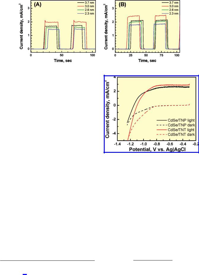
Figure 6. Photocurrent response of (A) OTE/TiO2(NP)/CdSe and (B) (Ti/TiO2(NT)/CdSe electrodes. Individual traces correspond to (a) 3.7, (b) 3.0, (c) 2.6, and (d) 2.3 nm diameter CdSe quantum dots anchored on nanostructured TiO2 films (excitation >420 nm, 100 mW/cm2; electrolyte, 0.1 M Na2S solution).
these spectra were recorded in the diffuse reflectance mode using blank OTE/TiO2(NP) or Ti/TiO2(NT) films as references. For comparison purposes, reported absorbance values shown in Figure 4 were converted directly from recorded reflectivity measurements.90 Our success in achieving relatively high coverage of CdSe quantum dots in these TiO2 films highlights the ability of small-sized CdSe quantum dots to penetrate the porous network of each TiO2 film and provide a uniform coverage throughout the film. Such monolayer coverage of the CdSe particles is analogous to mesoscopic TiO2 films modified with sensitizing dyes.91
Photoelectrochemistry of TiO2 Films Modified with CdSe Quantum Dots. The photoelectrochemical behavior of OTE/ TiO2(NP)/CdSe and Ti/TiO2(NT)/CdSe electrodes in terms of open circuit photovoltage and short-circuit current is presented in Figures 5 and 6, respectively. Upon illumination of the OTE/ TiO2/CdSe film with visible light, we observed prompt generation of anodic current similar to previous observations.65
An open circuit voltage of 650 ( 20 mV was observed for all eight electrodes following excitation with visible light (ì > 420 nm). The open-circuit potential is independent of CdSe particle size, indicating that electrons injected from excited CdSe into TiO2 quickly relax to the lowest conduction band energy. Hence, the conduction band level of TiO2 and the redox potential of the sulfide electrolyte alone dictate an open-circuit voltage of 600 mV.
The photocurrent response, however, varies with particle size (Figure 6). The maximum photocurrent is seen with 3.0 nm diameter CdSe particles. (Table S3 in the Supporting Information for a monochromatic response of the photocurrent generation.) Two opposing effects account for the difference in photocurrent generation at OTE/TiO2/CdSe electrodes. Decreasing particle size of CdSe increases photocurrent as the shift in the conduction band to more-negative potentials increases the driving force for charge injection. Transient absorption measurements reported in our earlier study48 support this observation. On the other hand, decreasing the CdSe particle size lowers photocurrent due to an inherently smaller response in the visible region.
We further evaluated the photoelectrochemical performance of both TiO2 particulate films and TiO2 nanotubes modified with
(90)Stone, F. S. In Surface Properties and Catalysis by Non-Metals Bonnelle, J. P., Delmon, B., Derouane, E. G., Eds.; Reidel, D. Publishing Company: New York, 1983; p 237.
(91)Meyer, G. J. Inorg. Chem. 2005, 44, 6852.
Figure 7. I-V characteristics of (A) OTE/TiO2(NP)/CdSe and (B) (Ti/ TiO2(NT)/CdSe electrodes (excitation >420 nm; intensity 100 mW/cm2; electrolyte, 0.1 M Na2S solution.)
3.0 nm diameter CdSe quantum dots by recording I-V characteristics (Figure 7). Both electrodes exhibited anodic photocurrent under applied electrochemical bias, confirming the primary role of the CdSe/TiO2 composite structure in dictating the overall photoelectrochemical behavior. As the electrodes were subjected to more-positive potentials, the charge collection and charge transport within the TiO2 network increased in efficiency. The similarity between the maximum photocurrent values seen under positive bias for these two electrodes shows that charge recombination during electron transport through TiO2 film is greatly minimized under applied potential.
Tuning the Photoelectrochemical Response through Size Quantization. The photoelectrochemical response of both OTE/ TiO2/CdSe films to monochromatic light irradiation was analyzed in terms of incident photon to charge carrier efficiency (IPCE). The IPCE was determined from short circuit photocurrents (Jshortcircuit) monitored at different excitation wavelengths (ì) using the expression,
1240 Jshortcircuit(A/cm2)
IPCE% ) ì(nm) Iincident(W/cm2) 100%
where Iincident is the energy of the monochromatic light incident
J. AM. CHEM. SOC. 9 VOL. 130, NO. 12, 2008 4011

A R T I C L E S |
Kongkanand et al. |
||
|
|
|
|
|
|
|
|
Figure 8. Photocurrent action spectra recorded in terms of incident photon to charge carrier generation efficiency (IPCE) of (A) OTE/TiO2(NP)/CdSe and
(B) (Ti/TiO2(NT)/CdSe electrodes. The individual IPCE responses correspond to (a) 3.7, (b) 3.0, (c) 2.6, and (d) 2.3 nm diameter CdSe quantum dots anchored on nanostructured TiO2 films.
on the electrode. The IPCE action spectra for OTE/TiO2(NP)/ CdSe and Ti/TiO2(NT)/CdSe electrodes are presented in Figure 8. The photocurrent action spectra obtained with 3.7, 3.0, 2.6, and 2.3 nm CdSe particles show similar trends for both films. The current peaks observed at 580, 540, 520, and 505 nm closely match the absorption plots in Figure 3. These observations confirm that the photocurrent generation at OTE/TiO2(NP)/CdSe and Ti/TiO2(NT)/CdSe electrodes originate from the individual CdSe quantum dots and their size quantization property is responsible for tuning the performance of quantum dot solar cells. In particular, the ability to tune the photoresponse by varying the size of CdSe particles affords the ability to tune the performance of quantum dot solar cells.
Comparison of IPCE at the excitonic peaks shows an interesting dependence on the particle size. The IPCE values measured at 580 nm (d ) 3.7 nm), 540 nm (d ) 3.0 nm), 520 nm (d ) 2.6 nm), and 505 nm (d ) 2.3 nm) were 14, 24, 26, and 28% for OTE/TiO2(NP)/CdSe and 19, 32, 35, and 36% for Ti/TiO2(NT)/CdSe, respectively. It should be noted that the absorbance at the excitonic band was matched to 0.73 ( 0.08. The difference in absorption (e5%) is smaller than the variation we see in the IPCE for these four electrodes. Hence, the strong dependence of IPCE on particle size is not due to the relatively small difference in absorption between the two electrodes. We consider the improved IPCE with smaller-sized quantum dots to arise from the improved rate of electron transfer. The smallersized particles, being more energetic in their excited state, are capable of injecting electrons into TiO2 at a faster rate. Although arguments have been made in the literature for the injection of hot electrons from the quantized semiconductor particles,69,92 we consider such a possibility under steady-state irradiation to be less likely. Careful analysis of the ultrafast kinetic measurements needs to be pursued to establish the contribution of hotelectron injection.
It is also interesting to note that the maximum IPCE obtained with CdSe quantum dots linked to TiO2 particles and tubes are different. The maximum IPCE values in the visible region (Figure 8) range from 25 to 35% for OTE/TiO2(NP)/CdSe electrodes, whereas they vary from 35 to 45% for OTE/Ti/TiO2- (NT)/CdSe electrodes. These IPCE values are relatively higher than those reported in the literature for the sensitization of TiO2 films (IPCE 25%)93 and ZnO nanorods (IPCE ) 18%)66 with CdSe quantum dots.93 (Note that the comparison made here is
based on IPCE or external quantum efficiency values and not based on light-harvesting efficiencies or APCE values.) Higher power-conversion efficiency has also been reported by Toyoda and co-workers67 using TiO2 inverse opal structures. These results demonstrate the necessity of optimizing nanostructure assemblies in an orderly fashion.
Although Figure 4 indicates that nanotube TiO2 films generally absorb more light than nanoparticle TiO2 films, this difference accounts for a no more than a 5% increase in overall photons absorbed. Comparing this with a 10% improvement in IPCE of the nanotube film over the nanoparticle film demonstrates the measurable advantage of a nanotube architecture for facilitating electron transport in nanostructure-based semiconductor films. The electrons in the particulate TiO2 films are more susceptible to loss at grain boundaries than those in nanotube TiO2 films. In addition, one also needs to take into consideration the role of crystal structure and surface defects between TiO2 tubes and particles during their interaction with CdSe quantum dots.
The open-circuit voltage recorded after stopping the illumination shows a slower decrease for Ti/TiO2(NT)/CdSe than for Ti/TiO2(NP)/CdSe electrodes (Figure 5). Under open-circuit conditions, electrons accumulate within the nanostructure semiconductor films following visible irradiation and shift the apparent Fermi level to negative potentials. Once the illumination is stopped, the accumulated electrons are slowly discharged because they are scavenged by the redox species in the electrolyte. The slower decay observed with tubular morphology is a further indication that the electrons injected from excited CdSe can survive longer and hence can facilitate electron transport without undergoing losses at grain boundaries. In agreement with recent studies that employ 1D nanostructure architecture, the results discussed here demonstrate the advantage of assembling semiconductor particles66,94-96 or lightharvesting assemblies75,76,97 on nanotube architecture for improving the photocurrent generation efficiency of solar cells.
(92)Rosenwaks, Y.; Thacker, B. R.; Nozik, A. J.; Ellingson, R. J.; Burr, K. C.; Tang, C. L. J. Phys. Chem. 1994, 98, 2739.
(93)Shen, Q.; Arae, D.; Toyoda, T. J. Photochem. Photobiol., A 2004, 164, 75.
(94)Olek, M.; Busgen, T.; Hilgendorff, M.; Giersig, M. J. Phys. Chem. B 2006, 110, 12901.
(95)Grzelczak, M.; Correa-Duarte, M. A.; Salgueirino-Maceira, V.; Giersig, M.; Diaz, R.; Liz-Marzan, L. M. AdV. Mater. 2006, 18, 415.
(96)Kongkanand, A.; DomõÂnguez, R. M.; Kamat, P. V. Nano Lett. 2007, 7, 676.
4012 J. AM. CHEM. SOC. 9 VOL. 130, NO. 12, 2008

Quantum Dot Solar Cells |
A R T I C L E S |
Figure 9. Emission spectra of 2.6 nm (a,b) and 3.7 nm (c,d) diameter CdSe quantum dot film deposited on glass (a,c) and OTE/TiO2(NP) films. Excitation was at 480 nm. Spectra b and d carry a multiplication factor of 3. All of the spectra were recorded using front face geometry.
Mechanistic Aspects of Charge Injection into TiO2 Particles. On the basis of the principle of sensitizing large-band- gap semiconductors with short-band-gap semiconductors, efforts have been made to employ short-band-gap semiconductors (e.g., CdS,17-19 PbS,20,21 Bi2S3,20,22 CdSe,23 and InP24) as sensitizers to extend the photoresponse of TiO2 into the visible region. CdSe quantum dots are capable of injecting electrons into the conduction band of TiO2 in a manner analogous to sensitizing dyes. The lower-lying conduction band of TiO2 (-0.5 V vs NHE) compared to quantized CdSe (e-1.0 V vs NHE) is expected to minimize the charge recombination and rectify the transport of charge carriers.23,57
The CdSe particles exhibit a band-edge emission peak, which also shifts to the blue region with decreasing particle size. Parts a and c of Figure 9 show the emission spectra of 2.6 and 3.7 nm CdSe quantum dots deposited on glass slides. These quantum dots exhibit characteristic emission peaks at 550 and 600 nm, respectively. When CdSe was anchored onto a TiO2 film (parts b and d of Figure 9), a significant quenching of the emission is seen, thus confirming the excited-state interaction between the two semiconductor particles. This quenching behavior represents the deactivation of the excited CdSe via electron transfer to TiO2 particles. The processes that follow the band-gap excitation of CdSe are presented in eqs 1-3:
CdSe +hî f CdSe (e + h) f CdSe +hî |
(1) |
CdSe (e) + TiO2 f CdSe + TiO2(e) |
(2) |
CdSe (h) + Red f CdSe + Ox |
(3) |
Whereas the electrons injected into TiO2 are collected to generate photocurrent, it is necessary to employ a redox couple to scavenge the holes (eq 3). Failure to scavenge holes could lead to surface oxidation, especially during extended periods of irradiation.98,99 In a typical photoelectrochemical cell, such oxidation is minimized by using a sulfide electrolyte.
(97)Hasobe, T.; Fukuzumi, S.; Kamat, P. V. J. Phys. Chem. B 2006, 110, 25477.
(98)Dimitrijevic, N. M. J. Chem. Soc., Faraday Trans. 1 1987, 83, 1193.
(99)Dimitrijevic, N. M.; Kamat, P. V. J. Phys. Chem. 1987, 91, 2096.
We further analyzed the excited CdSe deactivation by monitoring the emission decay. Figure 10 shows the emission decay recorded with 2.6 and 3.7 nm CdSe quantum dots. The emission decay was multiexponential because the distribution in the recombination rate constants influenced the decay kinetics. Triexponential decay kinetics were found to be satisfactory in the determination of emission lifetimes. These values were then used to estimate the average lifetime of CdSe emission decay using expression 4.100
a1ô12 + a2ô22 + a3ô32 |
|
áôñ ) a1ô1 + a2ô2 + a3ô3 |
(4) |
When deposited on a glass slide, 2.6 and 3.7 nm CdSe particles exhibited emission decays with average lifetimes of 4.1 and 7.9 ns, respectively. When anchored on TiO2 particles, the average time decreased to 0.4 and 1.3 ns for 2.6 and 3.7 nm diameter CdSe quantum dots, respectively. A similar decrease in the CdSe emission lifetime was also seen in the case of TiO2 nanotubes (Table 1).
If we assume that the observed decrease in lifetime is due to the charge transfer to TiO2, we can estimate the charge-transfer rate constant by the expression 5.
ket |
) |
1 |
|
- |
1 |
|
(5) |
ô(CdSe + TiO |
|
ô(CdSe) |
|||||
|
|
) |
|
||||
|
|
2 |
|
|
|
|
|
Using the lifetimes values listed in Table 1, we obtain electron-transfer rate constants of 2.5 109 and 0.63 109 s-1 respectively for 2.6 and 3.7 nm diameter CdSe quantum dots on particulate TiO2 films. Similar rate constants were also observed for TiO2 nanotubes. The similarity between the rate constant values observed for TiO2 particles and TiO2 nanotubes (Table 1) shows that the charge injection dynamics is dictated mostly by the energetics of quantized CdSe particles and not the morphology of the acceptor TiO2. The conduction band of TiO2 is at -0.5 V versus NHE.15 Larger CdSe particles with the bulk properties have band energies close to the reported value of -0.8 V versus NHE.101 The difference between the two conduction band energy levels serves as a driving force for the interparticle electron transfer (Scheme 2). Because the shift in the conduction band energy is significantly greater than the shift in valence band energy for quantized particles,42 we expect the conduction band of CdSe quantum dots to become more negative (on an NHE scale) with decreasing particle size. Thus, we see an increase of a factor of 2 in the charge injection rate constant when we employ 2.6 nm CdSe instead of 3.7 nm quantum dots.
In the dye sensitization of TiO2, it has been shown that the higher vacant energy levels of TiO2 facilitate direct electron transfer from the excited sensitizer in the subpicosecond time scale.102-105 However, in the present study we were not able to seek any evidence for hot electron transfer from the higher energy states. Thus, these rate constants represent electron
(100)James, D. R.; Liu, Y.-S.; de Mayo, P.; Ware, W. R. Chem. Phys. Lett. 1985, 120, 460.
(101)Wang, C. J.; Shim, M.; Guyot-Sionnest, P. Science 2001, 291, 2390.
(102)Ramakrishna, S.; Willig, F. J. Phys. Chem. B 2000, 104, 68.
(103)Tachibana, Y.; Haque, S. A.; Mercer, I. P.; Durrant, J. R.; Klug, D. R. J. Phys. Chem. B 2000, 104, 1198.
(104)Randy, J.; Ellingson, R. J.; Asbury, J. B.; Ferrere, S.; Ghosh, H. N.; Sprague, J. R.; Lian, T.; Nozik, A. J. J. Phys. Chem. B 1998, 102, 6455.
(105)Gaillard, F.; Sung, Y.-E.; Bard, A. J. J. Phys. Chem. B 1999, 103, 667.
J. AM. CHEM. SOC. 9 VOL. 130, NO. 12, 2008 4013

A R T I C L E S |
Kongkanand et al. |
||
|
|
|
|
|
|
|
|
Figure 10. Emission decay of (A) 2.6 nm (emission at 540 nm) and (B) 3.7 nm diameter (emission at 580 nm) CdSe quantum dots deposited on glass slide, TiO2 nanoparticulate film, and TiO2 nanotube array. The excitation wavelength was 457 nm. Solid lines represent the kinetic fit using triexponential decay analysis. The prompt measurement of instrument response used to mathematically deconvolute best-fit curve is also shown.
Table 1. Kinetic Parameters of the CdSe Emission Decay Analysisa
|
CdSe |
|
|
|
|
|
|
|
|
CdSe/ |
diameter |
|
|
|
|
|
|
|
ket, |
Film |
nm |
a1 |
ô1 ns |
a2 |
ô2 ns |
a3 |
ô3 ns |
<ô> ns |
(±0.2) 109 s-1 |
on glass |
2.6 |
0.679 |
0.330 |
0.058 |
2.39 |
0.0105 |
12 0.4 |
4.1 |
|
3.7 |
0.261 |
0.581 |
0.144 |
3.08 |
0.036 |
14.2 |
7.9 |
|
|
|
|
||||||||
on particulate/ |
2.6 |
0.529 |
0.148 |
3.002 |
0.501 |
0.0015 |
3.38 |
0.4 |
2.50 |
TiO2 (P) |
3.7 |
0.728 |
0.167 |
0.225 |
0.754 |
0.0423 |
3.11 |
1.3 |
0.63 |
on TiO2 |
2.6 |
1.299 |
0.169 |
0.102 |
0.620 |
0,0035 |
3.53 |
0.4 |
2.2 |
nanotubes (NT) |
3.7 |
1.217 |
0.178 |
0.238 |
0.753 |
0.0055 |
3.59 |
1.5 |
0.55 |
|
|
|
|
|
|
|
|
|
|
a See Table S2 in the Supporting Information for details on the decay analysis including standard deviation and chi-square values.
Scheme 2. Schematic Diagram Illustrating the Energy Levels of Different-Sized CdSe Quantum Dots and TiO2a
a The injection of electrons from CdSe quantum dots into TiO2 is influenced by the energy difference between the two conduction bands. (Note that band positions are for reference only and not drawn to scale.)
transfer between low-lying S-state of CdSe quantum dots and the conduction band of TiO2.
Toward the Design of Rainbow Solar Cells. The maximum photocurrents obtained with 3.0 nm CdSe particles were 2.0 and 2.4 mA/cm2 for OTE/TiO2(NP)/CdSe and Ti/TiO2(NT)/ CdSe electrodes under visible light irradiation (ì > 420 nm, 80 mW/cm2). The open-circuit photovoltage for these two electrodes were 600 and 580 mV, respectively. The fill factor for these photo electrochemical cells was estimated as 0.4. We estimate the overall power-conversion efficiency as 0.6 and 0.7% for OTE/TiO2(NP)/CdSe and Ti/TiO2(NT)/CdSe elec-
trodes, respectively. Although the net power-conversion efficiency of these electrodes is significantly lower than dyesensitized solar cells or organic solar cells, we consider the values obtained for quantum dot solar cells to be quite encouraging. Nearly 1% power-conversion efficiency reported in this study is our initial effort toward demonstrating the effectiveness of quantum dots as sensitizers for the next generation solar cells. By optimizing the cell configuration and improving the light absorption properties of the electrodes, it should be possible to further improve the performance of quantum dot solar cells.
One such approach under consideration is the construction of a rainbow solar cell, which employs an ordered assembly of CdSe nanoparticles of different diameters. An example of TiO2 nanotubes decorated with different-sized CdSe nanoparticles is shown in Scheme 3. As white light enters the cell, smallersized CdSe particles (larger band gap) absorb the portion of the light with smaller wavelengths (blue region). Light with longer wavelengths (red region), which is transmitted through the initial layer, is absorbed by subsequent layers, and so on. By creating an orderly gradient of quantum dots of different size, it should be possible to increase the effective capture of incident light.
As shown in the present study, smaller-sized particles exhibit higher photoconversion efficiency but absorb less light than larger-sized particles. If we can anchor the quantized particles on a nanotube array, it should be possible to maximize the capture of the incident light while collecting and transmitting electrons through the TiO2 tube network. It is true that the excess energy of electrons of small-sized particles is lost once they are transferred to TiO2 manifold; however, such a rainbow cell configuration allows one to couple the faster electron injection
4014 J. AM. CHEM. SOC. 9 VOL. 130, NO. 12, 2008

Quantum Dot Solar Cells |
A R T I C L E S |
Scheme 3. Artistic Impression of a Rainbow Solar Cell Assembled with Different-Sized CdSe Quantum Dots on a TiO2 Nanotube Array
rate of small-sized particles and greater absorption range of large particles effectively. Efforts are currently underway to construct such a rainbow solar cell and test its effectiveness in improving photoconversion efficiency.
Conclusions
By combining spectroscopic and photoelectrochemical techniques we have demonstrated size-dependent charge injection from different-sized CdSe quantum dots into TiO2 nanoparticles and nanotubes. The photoresponse and photoconversion ef-
ficiency of quantum dot solar cells are readily tuned by controlling the CdSe size. Smaller-sized CdSe quantum dots show greater charge injection rates and also higher IPCE at the excitonic band. Larger particles have better absorption in the visible region but cannot inject electrons into TiO2 as effectively as smaller-sized CdSe quantum dots. Because of the interplay of various factors, we observe maximum power-conversion efficiency (e1%) with 3 nm diameter quantum dots. The difference in TiO2 morphology has little effect on the charge injection rate but influenced the electron transport within the film. Maximum IPCE value (45%) obtained with CdSe/TiO2- (NT) is greater than that of CdSe/TiO2(NT) (35%). Tubular TiO2 architecture provides a better scaffold for the construction of quantum dot solar cells. Efforts are underway to construct rainbow solar cells to maximize the light absorption of quantum- dot-based solar cells.
Acknowledgment. The research described herein was supported by the Department of Energy, Office of Basic Sciences. We would like to thank Toyota Central R&D Labs., Inc., Aichi, Japan for the research grant for enabling T.K. to conduct research at Notre Dame. We also would like to thank James Puthussery for his help in synthesizing CdSe quantum dots. This is contribution number NDRL 4752 from the Notre Dame Radiation Laboratory.
Supporting Information Available: Roughness factor estimations, tables of kinetic analysis, photocurrent values, and ref 6. This material is available free of charge via the Internet at http://pubs.acs.org.
JA0782706
J. AM. CHEM. SOC. 9 VOL. 130, NO. 12, 2008 4015